
Input interface circuit

An input interface circuit and circuit technology, which is applied in the direction of logic circuit connection/interface layout, logic circuit coupling/interface using field effect transistors, etc., can solve the problem that the input interface circuit does not have anti-attack, and improve the anti-attack. Effect

Active Publication Date: 2015-05-20
SHANGHAI HUAHONG INTEGRATED CIRCUIT
View PDF5 Cites 1 Cited by
  • Summary
  • Abstract
  • Description
  • Claims
  • Application Information

AI Technical Summary

Problems solved by technology

[0009] Traditional input interface circuits are not resistant to attacks

Method used


Image

  • Input interface circuit
  • Input interface circuit
  • Input interface circuit

Examples


Embodiment Construction

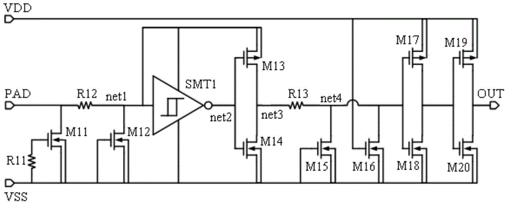
[0026] see figure 2 As shown, the input interface circuit of the present invention includes in the following embodiments:

[0027] An ESD protection circuit is composed of NMOS transistors M11 and M12, and resistors R11 and R12. Wherein, the NMOS transistor M11 and the resistor R11 are the main ESD protection circuit, which adopts a gate coupling structure. The resistor R12 is an ESD current-limiting resistor, and the NMOS transistor M12 is a secondary ESD protection circuit, protecting the gate of the subsequent circuit (Schmidt circuit).

[0028] The drain of the NMOS transistor M11 is connected to one end of the resistor R12 and serves as the input of the PAD, the gate of the NMOS transistor M11 is connected to one end of the resistor R11, and the other end of the resistor R11 is connected to the source and substrate of the NMOS transistor M11 grounded.

[0029] The other end of the resistor R12 is connected to the source of the PMOS transistor M12, and the node connect...


PUM


Abstract

The invention discloses an input interface circuit comprising an ESD (electro-static discharge) protection circuit, a waveshaping circuit, a well resistor circuit, an internal protection circuit and a buffer circuit. The ESD protection circuit includes a main ESD protection circuit and an auxiliary ESD protection circuit and prevents a chip from the damage made by external electrostatic discharge. The waveshaping circuit is composed of a Schmidt circuit and a buffer and connected with the ESD protection circuit. The Schmidt circuit is powered by an input PAD and used for shaping input signals. The well resistor circuit is connected with the waveshaping circuit and used for preventing an attacker from adding signals into the chip. The internal protection circuit is connected with the well resistor circuit and used for preventing voltage, caused during scribing, against damaging a circuit in the chip and allowing an output end of the input interface circuit outputting fixed low level as a resistor is cut off. The buffer circuit is connected with the internal protection circuit and used for strengthening drive capability of an input interface. The input interface circuit has the advantages that anti-attacking capability of the chip is remarkably improved, and accordingly the circuit in the chip is protected from damage of the attacker through the input PAD.

Description

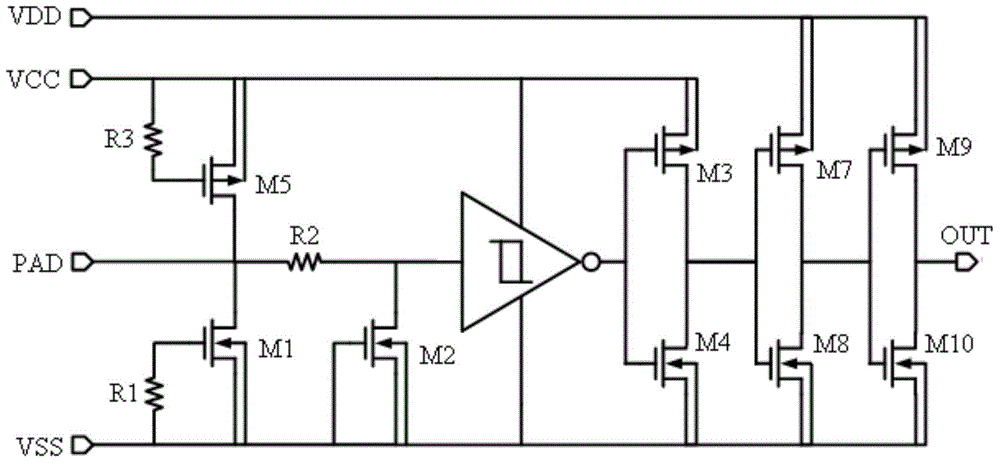
technical field [0001] The invention relates to the field of I / O interface circuits, in particular to an input interface circuit. Background technique [0002] With the rapid development of integrated circuit technology, chips are widely used in various industries, and chips used in the field of financial security put forward higher requirements for chip security. [0003] For chips with a higher security level, designers should not only care about the chip's security algorithm module but also the chip's interface. The interface circuit is directly connected to the outside world, so it is most vulnerable to attacks. Attackers can attack the chip through the I / O interface without destroying the chip. [0004] see figure 1 As shown, the traditional input interface circuit is composed of ESD protection circuit, Schmidt circuit and buffer circuit. [0005] The ESD protection circuit is an electrostatic discharge protection circuit, which can solve most of the electrostatic di...

Claims


Application Information

Patent Timeline
Patent Type & Authority Applications(China)
IPC IPC(8): H03K19/0175H03K19/0185
Inventor 范志祥舒海军
Owner SHANGHAI HUAHONG INTEGRATED CIRCUIT
Learn More