Organic light-emitting display device and manufacturing method thereof

A technology of light-emitting display and manufacturing method, applied in the field of display, can solve problems such as evaporation process offset, lower yield rate of AMOLED display panel, and display center of gravity imbalance, so as to achieve the effects of improving yield rate, avoiding color mixing phenomenon, and balancing center of gravity

Active Publication Date: 2015-05-27
WUHAN TIANMA MICRO ELECTRONICS CO LTD +1
View PDF5 Cites 14 Cited by
  • Summary
  • Abstract
  • Description
  • Claims
  • Application Information

AI Technical Summary

Problems solved by technology

[0004] Figure 1a It is a structural diagram of a pixel unit in an organic light-emitting display device in the prior art, see Figure 1a , since the areas of red sub-pixel R, blue sub-pixel B and green sub-pixel G in each pixel unit are equal, and compared with the other two sub-pixels, green sub-pixel G has the highest brightness, when AMOLED is displaying images There will be an unbalanced display center of gravity; in order to improve the unbalanced display center of gravity, in the prior art, two green sub-pixels G are set in one pixel unit to achieve (see Figure 1b ), however, in the process of manufacturing AMOLED, it is necessary to use a high-precision alignment system and a fine metal mask (Fine Metal Mask, FMM) to separately perform the red sub-pixel R, blue sub-pixel B and green sub-pixel G Evaporation, due to the limitation of FMM precision, it is easy to shift during the evaporation process, causing the organic light-emitting materials to be stacked on each other, causing color mixing of the AMOLED display panel, thereby reducing the yield of the AMOLED display panel

Method used


Image

  • Organic light-emitting display device and manufacturing method thereof
  • Organic light-emitting display device and manufacturing method thereof
  • Organic light-emitting display device and manufacturing method thereof

Examples


Embodiment Construction

[0032] The present invention will be further described in detail below in conjunction with the accompanying drawings and embodiments. It should be understood that the specific embodiments described here are only used to explain the present invention, but not to limit the present invention. In addition, it should be noted that, for the convenience of description, only parts related to the present invention are shown in the drawings but not all of them, and the same or similar symbols in the drawings represent the same or similar elements or have the same or similar functions components.

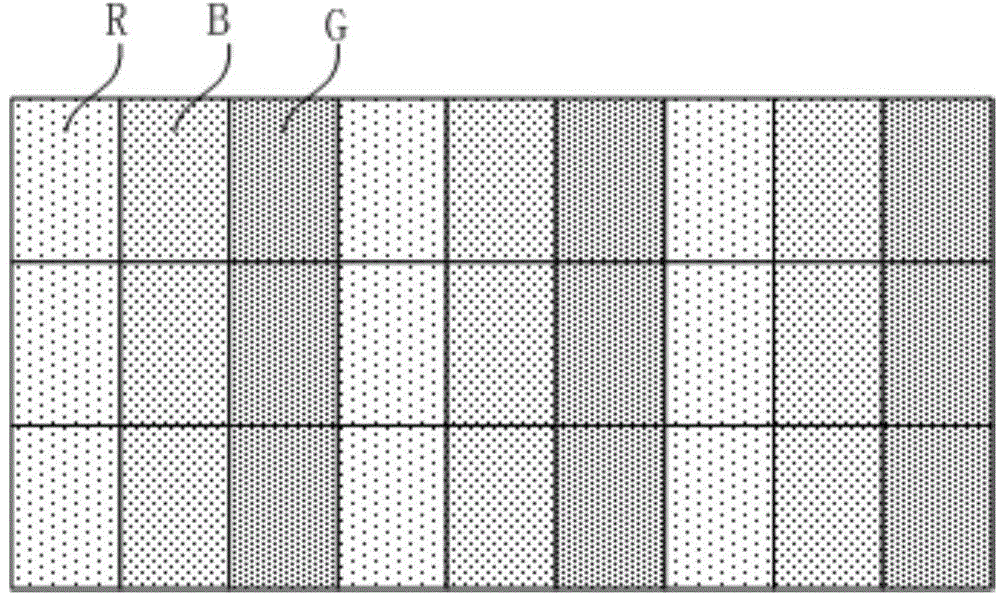
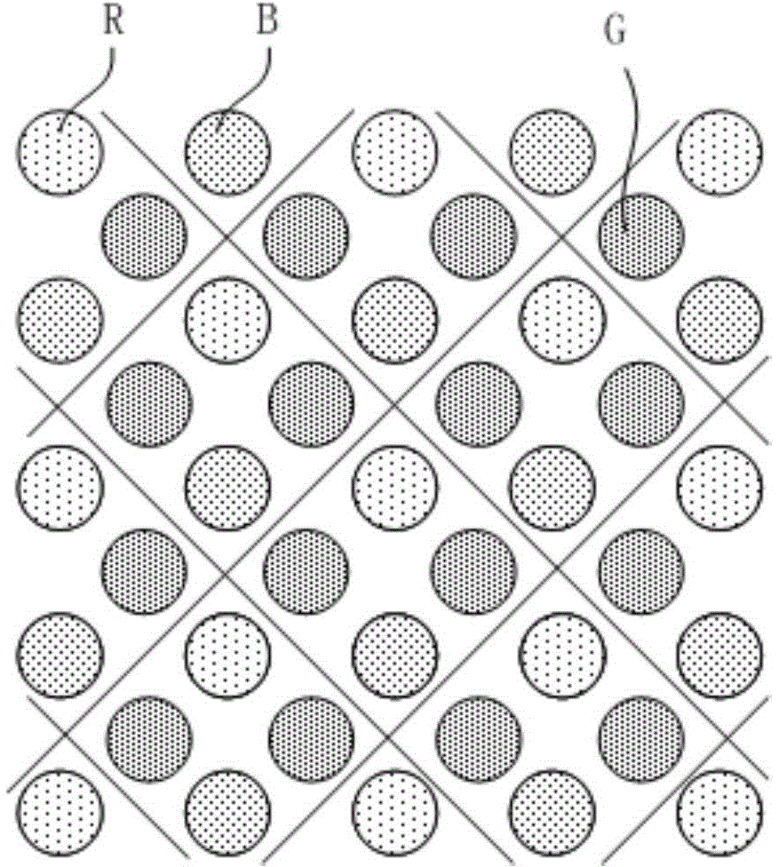
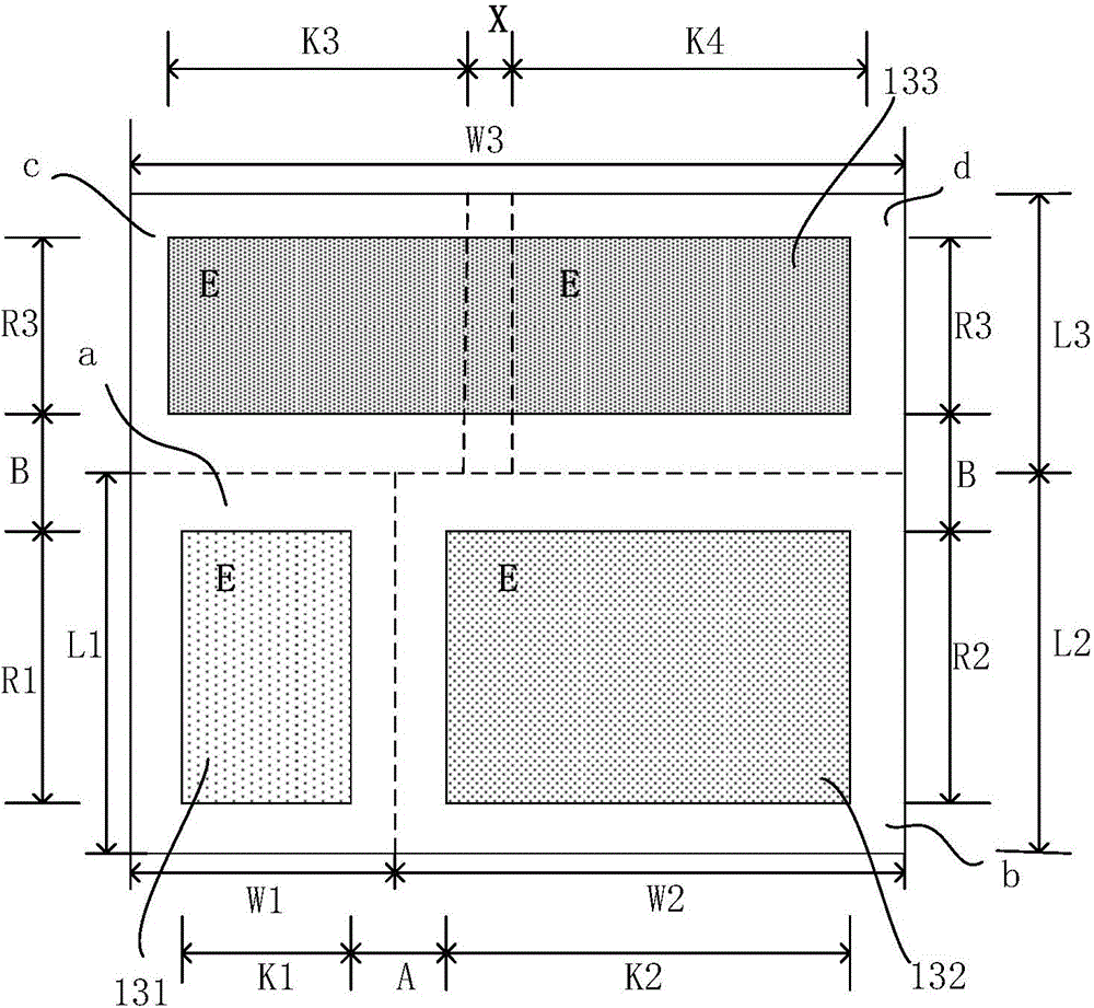
[0033] An embodiment of the present invention provides an organic light emitting display device, see figure 2 as well as Figure 3a and Figure 3b , figure 2 It is a top structural view of an organic light-emitting display device provided by an embodiment of the present invention; Figure 3a and Figure 3b It is a cross-sectional structure diagram of an organic light-emitting display d...


PUM


Abstract

The invention discloses an organic light-emitting display device and a manufacturing method thereof. The organic light-emitting display device comprises a substrate, pixel definition layers located on the substrate, first organic light-emitting layers, second organic light-emitting layers and third organic light-emitting layers, wherein multiple pixel units distributed together are defined by the pixel definition layers, each pixel unit comprises at least one first sub pixel, at least one second sub pixel and at least one third sub pixel, and each third sub pixel comprises at least two third auxiliary sub pixels; the first organic light-emitting layers are arranged in the at least one first sub pixel; the second organic light-emitting layers are arranged in the at least one second sub pixel, the third organic light-emitting layers are arranged in the at least two third auxiliary sub pixels and has a brightest light-emitting characteristic, and the third organic light-emitting layers arranged in the at least two third auxiliary sub pixels are connected together. According to the organic light-emitting display device and the manufacturing method thereof, the image display gravities of the organic light-emitting display device can be balanced, the color mixture phenomenon of an organic light-emitting display panel can be avoided, and accordingly, the yield of the organic light-emitting display device is increased.

Description

technical field [0001] The invention relates to the field of display technology, in particular to an organic light-emitting display device and a manufacturing method thereof. Background technique [0002] Organic Light-Emitting Diode (OLED) is a semiconductor device that can convert electrical energy into light energy. panel. According to different driving methods, OLEDs are further divided into active-matrix organic light emitting diodes (AMOLED) and passive-matrix organic light emitting diodes (passive-matrix organic light emitting diodes, PMOLED). [0003] The AMOLED display device includes a plurality of pixel units arranged in a matrix, and the pixel units include red sub-pixels R, blue sub-pixels B and green sub-pixels G, because the red sub-pixels R, blue sub-pixels B and green sub-pixels G correspond to The organic light-emitting materials used are different, so the red sub-pixel R, blue sub-pixel B, and green sub-pixel G have different luminous characteristics. Am...

Claims


Application Information

Patent Timeline
Patent Type & Authority Applications(China)
IPC IPC(8): H01L27/32H01L51/50H01L21/77H01L51/56H05B44/00
CPCH10K59/352H10K59/353H10K59/122H10K59/173
Inventor 李松黄盛俞凝罗丽媛吕博嘉
Owner WUHAN TIANMA MICRO ELECTRONICS CO LTD
Why Eureka
Try Eureka