Circuit board and circuit board manufacturing method

A circuit board manufacturing and circuit board technology, applied in the directions of printed circuit manufacturing, printed circuits, printed circuit components, etc., can solve problems such as disconnection, depression of electrical connection pads, and disconnection, so as to avoid disconnection and reduce disconnection. The effect of the possibility of the line

Inactive Publication Date: 2015-06-03
AVARY HLDG (SHENZHEN) CO LTD +1
View PDF5 Cites 5 Cited by
  • Summary
  • Abstract
  • Description
  • Claims
  • Application Information

AI Technical Summary

Problems solved by technology

Usually there is a gap between the conductive lines on the opposite side of the electrical contact pads used for wire bonding, which is easy to cause a gap when the cover film is pressed, so that part of the electrical connection pads are sunken after pressing, so that when punching When the chip is mounted on the wire, a disconnection occurs at the recess, which affects the electrical connection between the chip and the circuit board

Method used


Image

  • Circuit board and circuit board manufacturing method
  • Circuit board and circuit board manufacturing method
  • Circuit board and circuit board manufacturing method

Examples


Embodiment Construction

[0017] The circuit board and the manufacturing method of the circuit board provided by the technical solution will be further described in detail below with reference to the accompanying drawings and embodiments.

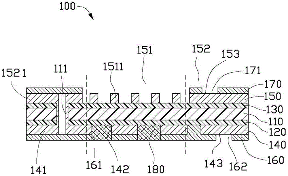
[0018] see figure 1 , the circuit board 100 provided by this technical solution includes a substrate 110 , a first adhesive layer 120 , a second adhesive layer 130 , a first conductive circuit layer 140 , a second conductive circuit layer 150 , a first cover film 160 , and a second cover film 170 And solder mask ink 180.

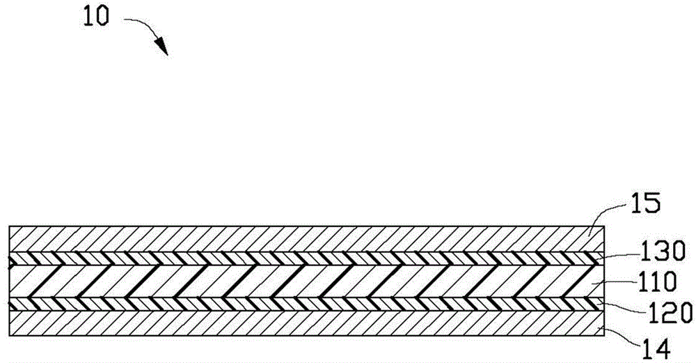
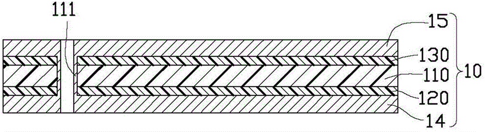
[0019] The substrate 110 includes a dielectric layer and an inner conductive circuit layer. The number of the dielectric layers is at least one. The number of the inner conductive circuit layers is one less than the number of dielectric layers. The dielectric layer and the inner conductive circuit layer are arranged at intervals. The adjacent inner conductive circuit layers are electrically connected through conductive holes in the dielectric ...


PUM


Abstract

The invention relates to a circuit board, which comprises a substrate, a first conductive line layer, a second conductive line layer, a first covering film and solder resist ink, wherein the first conductive line layer and the second conductive line layer are arranged at two opposite sides of the substrate; the second conductive line layer is provided with a connection area; the connection area is internally distributed with multiple electrical contact pads; the first conductive line layer comprises multiple first conductive lines; multiple gaps exist between the first conductive line layer and the first conductive lines in the region corresponding to the connection area; the first covering film covers the first conductive line layer; the region in the connection area corresponding to the first covering film is provided with multiple openings; the first openings and the gaps are in one-to-one correspondence so as to enable corresponding gaps to be exposed; and the solder resist ink fills the multiple first openings and the multiple gaps. The invention also relates to a circuit board manufacturing method.

Description

technical field [0001] The invention relates to a circuit board manufacturing technology, in particular to a circuit board and a circuit board manufacturing method. Background technique [0002] With the gradual thinning of electronic products, the application of directly mounting chips on circuit boards has gradually increased. Usually, there is a gap between the conductive lines on the back side of the electrical contact pads for wire bonding, which is easy to cause a break when the cover film is pressed, so that some of the electrical connection pads are recessed after pressing, so that the When the chip is mounted by wire, a wire break occurs in the recess, which affects the electrical connection between the chip and the circuit board. SUMMARY OF THE INVENTION [0003] In view of this, it is necessary to provide a circuit board and a manufacturing method of the circuit board. [0004] A circuit board includes a substrate, a first conductive circuit layer, a second co...

Claims


Application Information

Patent Timeline
Patent Type & Authority Applications(China)
IPC IPC(8): H05K1/02H05K3/00
CPCH05K1/0298H05K3/465H05K2203/063
Inventor 周琼
Owner AVARY HLDG (SHENZHEN) CO LTD
Why Eureka
Try Eureka