Array substrate and liquid crystal display device

A technology for array substrates and display areas, which is applied in the direction of instruments, semiconductor devices, optics, etc., can solve problems such as electrostatic breakdown of devices, and achieve the effect of reducing static electricity

Inactive Publication Date: 2015-06-10
SHANGHAI TIANMA MICRO ELECTRONICS CO LTD +1
View PDF6 Cites 20 Cited by
  • Summary
  • Abstract
  • Description
  • Claims
  • Application Information

AI Technical Summary

Problems solved by technology

[0005] In view of this, the present invention provides an array substrate and a liquid crystal display device, which effectively solves the problem of electrostatic breakdown of devices

Method used


Image

  • Array substrate and liquid crystal display device
  • Array substrate and liquid crystal display device
  • Array substrate and liquid crystal display device

Examples


Embodiment Construction

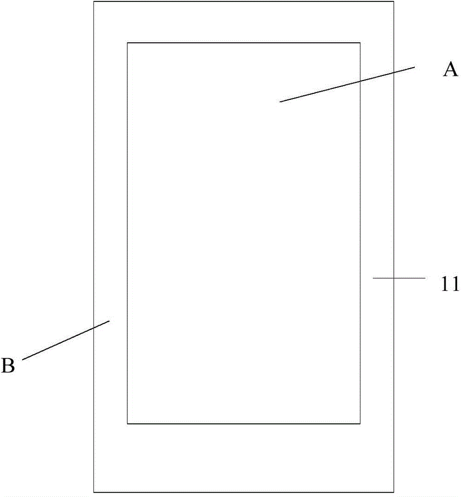
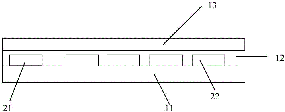
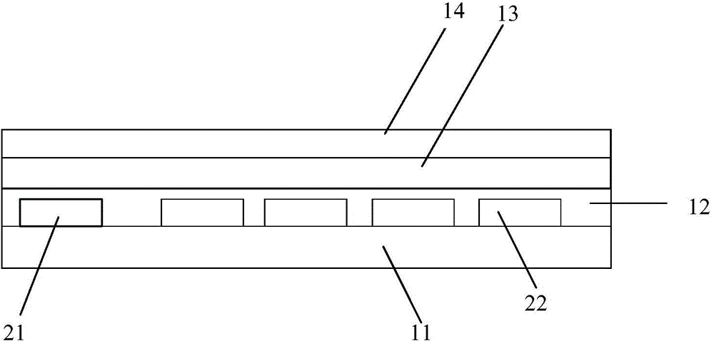
[0033] The present invention provides an array substrate, comprising: a substrate, wherein the substrate has a display area and a wiring area surrounding the display area, and a wiring layer is provided in the wiring area on the surface of the substrate, and the wiring layer An insulating protective layer is provided on the insulating protective layer. In addition, an electrostatic protective layer is provided on the insulating protective layer. It can be seen that the array substrate provided by the present invention does not need to connect capacitors at both ends of the ground wire to reduce static electricity, and occupies a small space and is effective. It solves the problem that the device is broken down by static electricity.

[0034] It should be noted that the electrostatic protection layer provided in this embodiment can be grounded by adding wires, or can be connected to the existing ground wire through via holes. Of course, no matter which method is used, as long a...


PUM


Abstract

The invention provides an array substrate. The array substrate comprises a substrate body with a display area and a lead area surrounding the display area. The lead area on the surface of the substrate body is provided with a wiring layer, and an insulating protection layer is arranged on the wiring layer. In addition, an electrostatic protection layer is arranged on the insulating protection layer. The array substrate has the advantages that connection of capacitors to two ends of a ground wire to reduce static electricity is not needed, little space is occupied, and the problem of electrostatic breakdown of devices is solved effectively.

Description

technical field [0001] The present invention relates to the field of display technology, and more specifically, to an array substrate and a liquid crystal display device. Background technique [0002] Liquid crystal displays are widely used in electronic products such as computer screens, mobile phones, and flat-screen TVs because of their thin and light appearance, power saving, and no radiation. Specifically, the liquid crystal display includes a liquid crystal panel, and the liquid crystal panel is composed of an array substrate, a color filter substrate, and liquid crystal encapsulated between the two substrates. [0003] Initially, the array substrate is usually externally connected with a driver chip made of silicon wafers, but currently, a gate driver IC is usually integrated and fabricated on the gate line lead area of ​​the array substrate. Specifically, the Amorphous Silicon Gate driver (ASG) can be integrated with the active matrix display, that is, the gate driv...

Claims


Application Information

Patent Timeline
Patent Type & Authority Applications(China)
IPC IPC(8): G02F1/1362
CPCG02F1/1362G02F1/136204G02F1/136286G02F1/136218H01L27/1255H01L27/0288H01L27/124
Inventor 孙云刚金慧俊李谷骏
Owner SHANGHAI TIANMA MICRO ELECTRONICS CO LTD
Why Eureka
Try Eureka