Phosphorus, arsenic and antimony co-doped N-type heavily-doped Czochralski silicon single crystal and silicon epitaxial wafer thereof

A technology of Czochralski silicon single crystal and co-doping, which is applied in the direction of single crystal growth, single crystal growth, crystal growth, etc., can solve the problems of semiconductor device yield loss, epitaxial lattice mismatch, etc., and achieve the elimination of mismatch Effect of Miswire Defect

Active Publication Date: 2015-06-17
ZHEJIANG QL ELECTRONICS
View PDF12 Cites 5 Cited by
  • Summary
  • Abstract
  • Description
  • Claims
  • Application Information

AI Technical Summary

Problems solved by technology

[0005] Continuing to increase the concentration of doping elements in N-type heavily doped Czochralski silicon single crystals using phosphorus or arsenic as dopants alone (reducing the resistivity of silicon single crystals) will encounter the problem of severe epitaxial lattice mismatch , the semiconductor device yield loss caused by the lattice mismatch of such Czochralski silicon single-crystal processed epitaxial wafers becomes unacceptable

Method used


Image

  • Phosphorus, arsenic and antimony co-doped N-type heavily-doped Czochralski silicon single crystal and silicon epitaxial wafer thereof

Examples


preparation example Construction

[0027] The preparation method of the N-type heavily doped Czochralski silicon single crystal co-doped with phosphorus, arsenic and antimony has the following steps:

[0028]1) Melting of polysilicon: Put the quartz crucible into the Czochralski silicon single crystal furnace, then fill the quartz crucible with polysilicon, vacuumize it, and melt the polysilicon with electricity, adjust the input power to stabilize the temperature of the silicon melt at 1460±20 ℃;

[0029] 2) Add phosphorus as the main doping element: put the weighed red phosphorus into the quartz cup, then hang the quartz cup in the quartz bell jar, and hang the quartz bell jar on the seed clamp of the pulling room of the silicon single crystal furnace On the head, vacuumize, open the isolation valve at the lower part of the lifting chamber, and lower the quartz bell jar to a position 5-10 mm away from the surface of the silicon melt in the quartz crucible to completely volatilize the dopant and be absorbe...


PUM

PropertyMeasurementUnit
diameteraaaaaaaaaa

Abstract

The invention discloses a phosphorus, arsenic and antimony co-doped N-type heavily-doped Czochralski silicon single crystal and a silicon epitaxial wafer thereof. The phosphorus, arsenic and antimony co-doped N-type heavily-doped Czochralski silicon single crystal takes phosphorus as the main doping element, and either or both of arsenic and antimony as auxiliary doping elements, the concentration of phosphorus is larger than or equal to 4.6*10<19> / cm<3>, phosphorus accounts for more than or equal to 60% of the doping elements, and the auxiliary doping elements accounts for 0.1-40% of the doping elements. The phosphorus, arsenic and antimony co-doped N-type heavily-doped Czochralski silicon single crystal can eliminate or remarkably reduce slip lines caused by lattice mismatching in the silicon epitaxial wafer, and can effectively reduce or eliminate mismatched dislocation lines generated when an epitaxial layer is grown on a polished wafer formed by processing of the N-type heavily-doped Czochralski silicon single crystal with high doping concentration; while the problems are solved, widening of a transition zone in a semi-conductor device after a high-temperature process is prevented; the industry practice that two or more of phosphorus, arsenic and antimony in a silicon single crystal cannot serve as dopants at the same time is changed.

Description

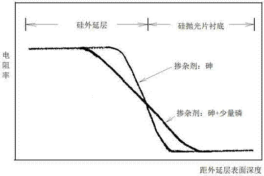
technical field [0001] The invention relates to the field of Czochralski silicon single crystal. Background technique [0002] The heavily arsenic-doped Czochralski silicon single crystal with arsenic as the main doping element (the concentration of arsenic is 1.2×10 19 -3.4×10 19 / cm 3 ) into a polished silicon wafer, and then manufacture the polished wafer into an epitaxial wafer with an epitaxial resistivity greater than 1Ω.cm. After the epitaxial wafer undergoes high-temperature processing of semiconductor devices, the distribution of the epitaxial layer resistivity in the vertical surface direction is as follows: figure 1 shown. The region where the resistivity between the silicon epitaxial layer and the polished substrate changes from high to low is called the epitaxial transition region. If the polished substrate contains a small amount of phosphorus in addition to arsenic, the corresponding epitaxial transition zone is wider than that corresponding to the...

Claims


Application Information

Patent Timeline
Patent Type & Authority Applications(China)
IPC IPC(8): C30B29/06C30B15/04
CPCC30B15/04C30B29/06
Inventor 田达晰马向阳李刚何永增郑铁波梁兴勃陈华王震
Owner ZHEJIANG QL ELECTRONICS
Why Eureka
Try Eureka