A method for preparing silicon nanostructure material under alternating electric field

A technology of alternating electric field and structural materials, applied in nanotechnology, chemical instruments and methods, crystal growth, etc., can solve the problems of low preparation efficiency, low structural accuracy of silicon nanostructured materials, and inability to prepare silicon nanostructured materials. , to improve the directional corrosion rate, facilitate electron transfer, and maintain the effect of concentration uniformity

Inactive Publication Date: 2017-07-04
HANGZHOU DIANZI UNIV
View PDF10 Cites 0 Cited by
  • Summary
  • Abstract
  • Description
  • Claims
  • Application Information

AI Technical Summary

Problems solved by technology

However, there are technical problems such as the inability to prepare complex silicon nanostructure materials and the low structural accuracy and low preparation efficiency of the prepared silicon nanostructure materials in the prior art.

Method used


Image

  • A method for preparing silicon nanostructure material under alternating electric field
  • A method for preparing silicon nanostructure material under alternating electric field
  • A method for preparing silicon nanostructure material under alternating electric field

Examples


Embodiment 1

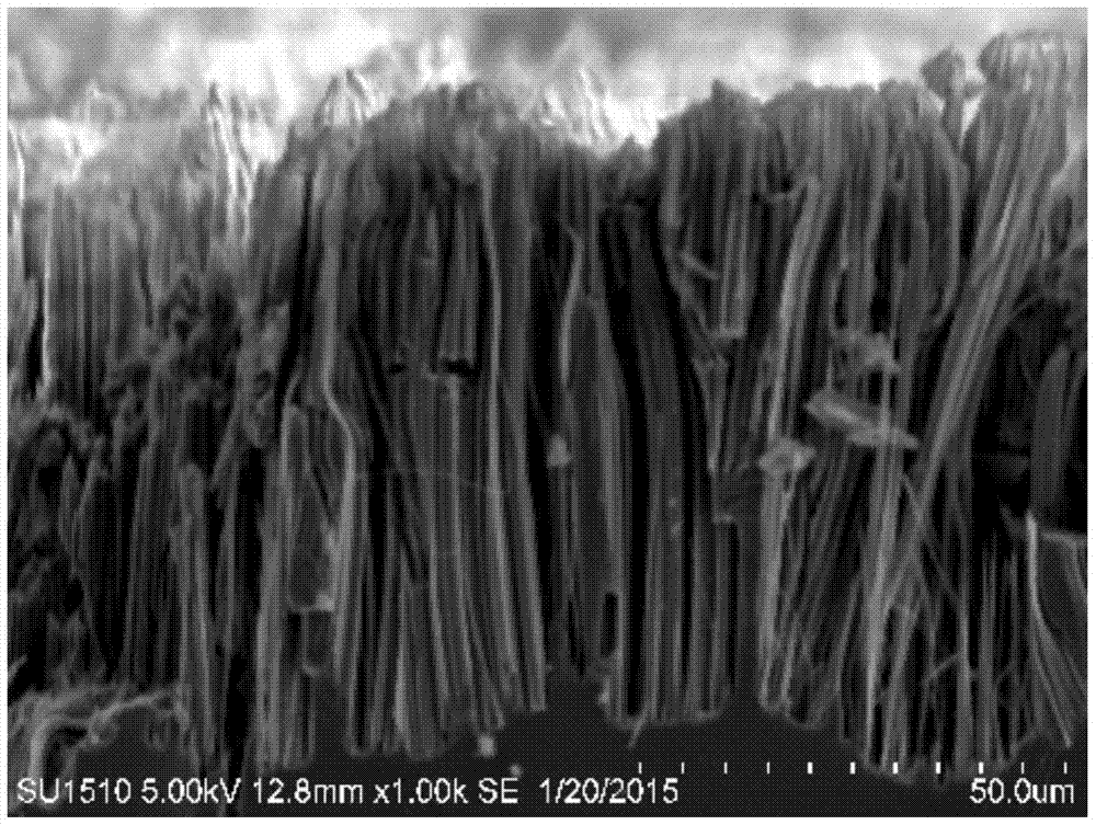
[0028] Embodiment 1, preparation silicon nanowire

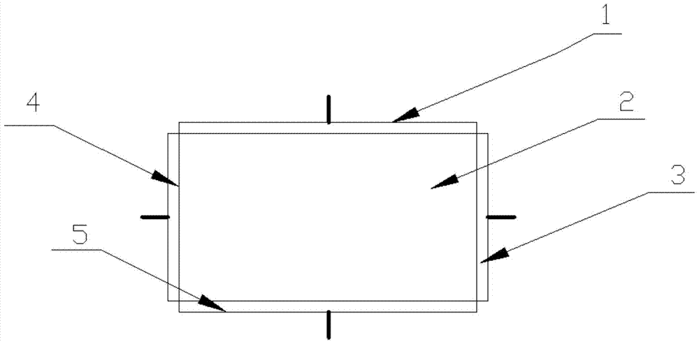
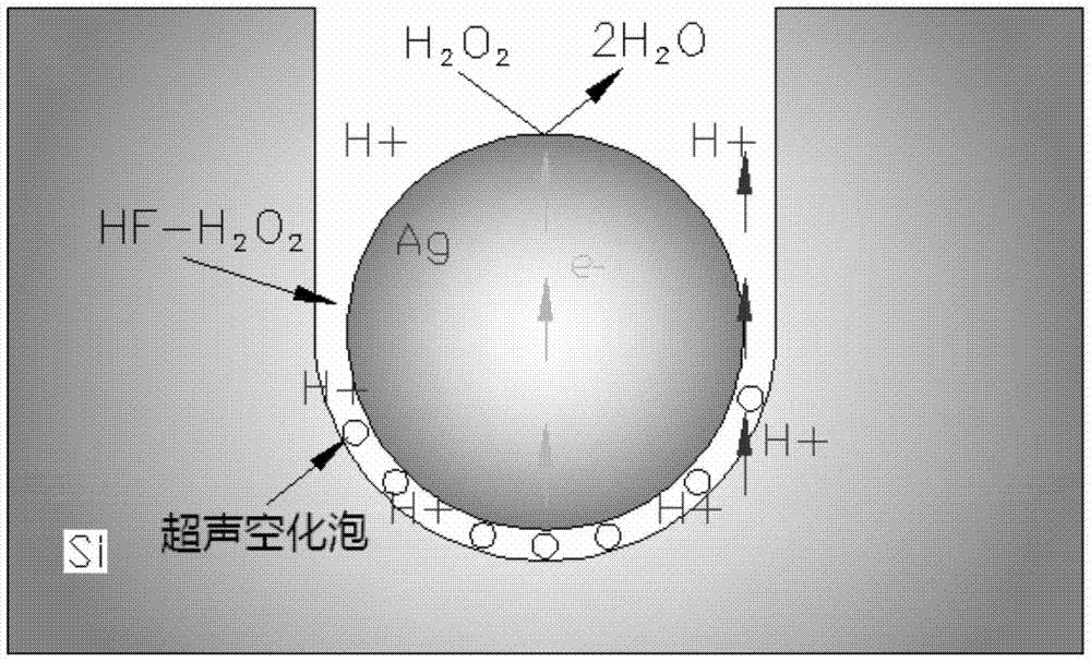
[0029] Put the clean bulk silicon and the pasted inert electrode into the corrosion solution. The composition ratio of the corrosion solution is hydrofluoric acid: hydrogen peroxide: silver nitrate: water, and the volume ratio is 12:1:1:36. Three pairs of inert electrodes are connected, the electric field strength is 300v / m-1000v / m, and the frequency is 40kHz; after being corroded for 120min at 15°C-25°C, it is taken out and cleaned to prepare a silicon nanowire structure.

Embodiment 2

[0030] Embodiment 2, preparation silicon nanowire

[0031] Put the clean bulk silicon and the pasted inert electrode into the corrosion solution. The composition ratio of the corrosion solution is hydrofluoric acid: hydrogen peroxide: silver nitrate: water, and the volume ratio is 12:1:1:36. Three pairs of inert electrodes are connected, the electric field strength is 300v / m-1000v / m, and the frequency is 40kHz; after being corroded for 120min at 15°C-25°C, it is taken out and cleaned to prepare a silicon nanowire structure.

Embodiment 3

[0032] Embodiment 3, preparation of 3D nano-silicon structure (arc structure prepared inside bulk silicon)

[0033] Put the clean bulk silicon and the pasted inert electrode into the corrosion solution. The composition ratio of the corrosion solution is hydrofluoric acid: hydrogen peroxide: silver nitrate: water, and the volume ratio is 10:1:1:38. Three pairs of inert electrodes are turned on at the same time, and the three electric field strengths are 300v / m-1000v / m respectively, and the frequency is 28kHz; after being corroded for 90min at 15°C-25°C, they are taken out and cleaned to prepare a 3D nano-silicon structure.


PUM

PropertyMeasurementUnit
diameteraaaaaaaaaa

Abstract

The invention discloses a method for preparing a silicon nanostructure material under alternative electric fields. The method comprises the following steps: 1, bonding six surfaces of bulk silicon with three pairs of independent inert electrodes, and drilling each of the inert electrodes with a fabrication hole, wherein the inert electrodes can generate alternative electrode fields; 2, putting the bulk silicon obtained in step 1 in a corrosive solution prepared by using hydrofluoric acid, hydrogen peroxide, a metal catalyst and deionized water; and 3, starting the inert electrodes after step 2, controlling the corrosion direction and the corrosion speed under three orthogonal alternative electric fields generated by the three inert electrodes under the frequency of the alternative electric fields of 28-40kHz, taking out the obtained bulk silicon after corrosion for a period of time, and cleaning to prepare the silicon nanostructure material. The method solves the problems of low metal assisted corrosion and low precision of the prepared silicon nanostructure, and controls the corrosion direction through the accurate control of metal catalyst particles by the alternative electric fields in order to realize accurate preparation of the three dimensional silicon nanostructure.

Description

technical field [0001] The invention belongs to the technical field of preparing silicon nanostructure materials, and in particular relates to a method for preparing silicon nanostructure materials under an alternating electric field. Background technique [0002] Silicon nanostructure materials play a very important role in the semiconductor industry, sensors, solar cells, MEMS and other fields. At present, the methods for preparing silicon nanostructure materials mainly include metal-catalyzed vapor-liquid-solid (VLS) method, solid-liquid-solid (SLS) growth method, plasma etching method, and metal-assisted chemical etching method. Among them, the metal-assisted chemical corrosion method has been widely recognized and applied internationally due to its advantages of simple operation and no need for precision equipment. Other methods also have their own advantages. However, in the prior art, there are technical problems such as inability to prepare complex silicon nanostru...

Claims


Application Information

Patent Timeline
Patent Type & Authority Patents(China)
IPC IPC(8): C30B33/04C30B33/10B82Y40/00
Inventor 巢炎焦晓东吴立群张俐楠林志朋叶玅宏
Owner HANGZHOU DIANZI UNIV
Why Eureka
Try Eureka