Method for manufacturing local-thick-copper circuit board and local-thick-copper circuit board

A technology of local thick copper and production method, applied in the production of local thick copper circuit boards and the field of local thick copper circuit boards, can solve the problems of prone to film lamination, high cost, over-corrosion, etc., so as to avoid film lamination and maintain thickness. Consistency, avoid over-corrosion or under-corrosion effect

Inactive Publication Date: 2015-06-17
SHENNAN CIRCUITS
View PDF7 Cites 7 Cited by
  • Summary
  • Abstract
  • Description
  • Claims
  • Application Information

AI Technical Summary

Problems solved by technology

[0006] The embodiment of the present invention provides a method for making a local thick copper circuit board and a local thick copper circuit board to solve the problem that the cost of the existing buried copper technology is too high and the existing local thick copper technology is prone to sandwiching, over-corrosion or undershooting. corrosion problem

Method used


Image

  • Method for manufacturing local-thick-copper circuit board and local-thick-copper circuit board
  • Method for manufacturing local-thick-copper circuit board and local-thick-copper circuit board
  • Method for manufacturing local-thick-copper circuit board and local-thick-copper circuit board

Examples


Embodiment 1

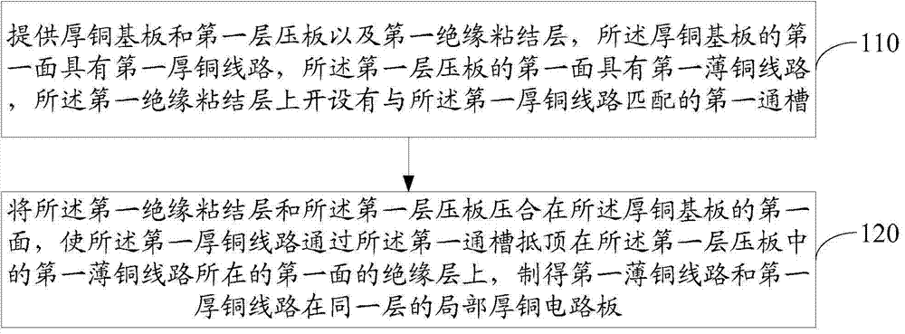
[0031] Please refer to figure 1 , an embodiment of the present invention provides a method for manufacturing a local thick copper circuit board, which may include:

[0032] 110. Provide a thick copper substrate, a first laminate and a first insulating bonding layer, the first surface of the thick copper substrate has a first thick copper circuit, and the first surface of the first laminate has a first thin copper For wiring, a first through-groove matching the first thick copper wiring is opened on the first insulating adhesive layer.

[0033] For thick copper lines and thin copper lines belonging to the same layer but with different thicknesses in the design scheme, the existing technology is to use the process of partial electroplating thickening or local etching thinning on the same metal layer of the copper clad laminate, but it is inevitable There will be problems such as film trapping, over-corrosion or under-corrosion.

[0034] In the embodiment of the present inventi...

Embodiment 2

[0066] Please refer to Figure 7 , an embodiment of the present invention provides a method for manufacturing a local thick copper circuit board, which may include:

[0067] 710. Provide a thick copper substrate, an insulating adhesive layer and a metal layer, one side of the thick copper substrate has a thick copper circuit, and the insulating adhesive layer and the metal layer have slots matching the thick copper circuit.

[0068] In this embodiment, a thick copper substrate with corresponding copper thickness is provided according to the thickness of the thick copper circuit to be formed; a metal layer with a corresponding thickness is provided according to the thickness of the thin copper circuit to be formed; according to the thickness of the thick copper circuit and the thin copper circuit, The difference in thickness provides an insulating bonding layer of corresponding thickness. Generally, the thickness of thick copper lines can be above 5OZ or 8OZ; the thickness of ...

Embodiment 3

[0109] Please refer to Figure 10 , an embodiment of the present invention provides a method for manufacturing a local thick copper circuit board, which may include:

[0110] 1010. Etch the first surface of the metal layer, wherein the non-circuit pattern part of the thick copper circuit area and the thin copper circuit area are etched to reduce the thickness.

[0111] In the embodiment of the present invention, thick copper lines and thin copper lines are fabricated on the metal layer by performing double-sided etching on the metal layer. Said metal layer can specifically be thicker copper foil layer or copper plate, etc., and its thickness can be more than 0.35 mm, or more than 10 OZ (ounce, 1 ounce is about 35 microns). In this embodiment, assuming that the thicknesses of the thick copper circuit and the thin copper circuit are required to be 10OZ and 5OZ respectively, then a metal layer of the same thickness can be blanked according to the size of the required thick coppe...


PUM


Abstract

The invention discloses a method for manufacturing a local-thick-copper circuit board and the local-thick-copper circuit board. The problems that an existing copper embedding technology is too high in cost, and an existing local-thick-copper technology is prone to film clamping, over etching or insufficient etching can be solved. The method includes the steps of etching the first face of a metal layer, wherein a non-circuit-pattern part of a thick copper circuit area and a thin copper circuit area are etched to be thinned; pressing an insulating layer on the first face of the metal layer; etching the second face of the metal layer, wherein a non-circuit-pattern part of the thin copper circuit area is etched to be removed to form a thin copper circuit, and the non-circuit-pattern part of the thick copper circuit area is etched to be removed to form a thick copper circuit.

Description

[0001] This application claims the priority of the Chinese patent application filed on December 12, 2013 with the application number 201310684084.0 and the title of the invention "A Method for Making Partially Thick Copper Circuit Board" with the China Patent Office, the entire contents of which are hereby incorporated by reference In this application. technical field [0002] The invention relates to the technical field of circuit boards, in particular to a method for manufacturing a partially thick copper circuit board and the partially thick copper circuit board. Background technique [0003] At present, in products such as high-power power supplies, the high-current circuit tends to be integrated on the circuit board for carrying, that is, the circuit board simultaneously carries high-current and ordinary signals. Usually, the existing circuit integration method adopts two technologies of buried copper and partial thick copper, and the buried copper or partial thick copp...

Claims


Application Information

Patent Timeline
Patent Type & Authority Applications(China)
IPC IPC(8): H05K3/46H05K1/00
CPCH05K1/00H05K3/02H05K3/107H05K3/46H05K3/4614H05K2201/0367
Inventor 沙雷崔荣刘宝林
Owner SHENNAN CIRCUITS
Why Eureka
Try Eureka