Supercharge Your Innovation With Domain-Expert AI Agents!

Organic image sensor and forming method thereof

An image sensor, an organic technology, applied in the field of image sensors, can solve the problems of limiting the absorption of incident light, organic image sensors need to be further improved, etc.

Active Publication Date: 2015-06-24
SEMICON MFG INT (SHANGHAI) CORP
View PDF5 Cites 5 Cited by
  • Summary
  • Abstract
  • Description
  • Claims
  • Application Information

AI Technical Summary

Problems solved by technology

[0005] 2. The structure and design of the traditional sensor limit the absorption of incident light, while the organic image sensor can absorb all the light reaching the sensor, which makes its photosensitivity 1.2 times higher than that of the traditional sensor, even in low light. get a clean screen
[0006] 3. The silicon photodiode in the silicon-based CMOS image sensor has a minimum thickness of 3 microns, which limits its incident light angle to only 30-40 degrees
[0007] However, the performance of existing organic image sensors still needs to be further improved

Method used


Image

  • Organic image sensor and forming method thereof
  • Organic image sensor and forming method thereof
  • Organic image sensor and forming method thereof

Examples


Embodiment Construction

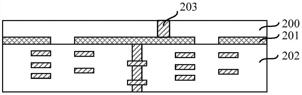
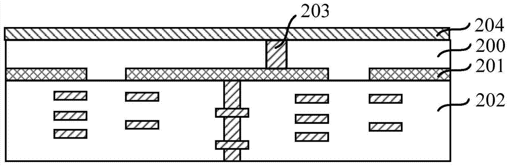
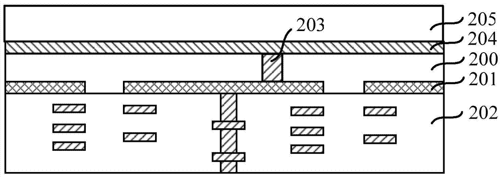
[0035] After research, the structure of the existing organic image sensor includes: a substrate, several discrete pixel lower electrodes located on the substrate; an organic photoelectric conversion layer located on the pixel lower electrode; and an upper electrode located on the organic photoelectric conversion layer. When external light is incident from above the upper electrode, the organic photoelectric conversion layer induces the light to generate charges, and receives the induced charges through the upper electrode and the corresponding lower electrode of the pixel. However, since the existing organic photoelectric conversion layer has a whole-layer structure, interference between adjacent pixel units is likely to occur when sensing light, and when external light is incident at a certain oblique angle, the incident light above a certain pixel unit The light will also irradiate into the organic photoelectric conversion layer corresponding to the adjacent pixel unit, there...


PUM


Abstract

The invention discloses an organic image sensor and a forming method thereof. The organic image sensor comprises a semiconductor substrate, a plurality of independent organic photoelectric converting layers and upper electrodes. The semiconductor substrate comprises a first surface and a second surface opposite to the first surface. Pixel circuits are formed on the first surface of the semiconductor substrate. A plurality of pixel lower electrodes distributed in a matrix mode are formed on the second surface of the semiconductor substrate. Each pixel lower electrode is connected with the corresponding pixel circuit through a through hole interconnection structure in the semiconductor substrate. The organic photoelectric converting layers are located on the second surface of the semiconductor substrate. Each organic photoelectric converting layer covers the corresponding pixel lower electrode. An isolation layer is arranged between every two adjacent organic photoelectric converting layers and the corresponding adjacent pixel lower electrodes. Each upper electrode is located on the corresponding organic photoelectric converting layer. According to the organic image sensor, interference between the adjacent pixel units is small, and dark current is prevented from being generated.

Description

technical field [0001] The invention relates to the field of image sensors, in particular to an organic image sensor and a forming method thereof. Background technique [0002] Image sensors have been widely used in cameras, medical equipment, cellular phones, automobiles, and others. The existing relatively common image sensor is a silicon-based CMOS (complementary metal oxide semiconductor) image sensor (CIS). Each pixel of a silicon-based image sensor typically includes a light-sensing element, such as a photodiode, and one or more transistors for reading signals from the light-sensing element. However, with the continuous innovation of technology, the continuous progress of society and the continuous improvement of sensor performance, the existing silicon-based CMOS sensors cannot meet the needs of existing applications. Therefore, the industry has proposed a new type of sensor-organic image sensors. Sensor (organic photoconductive image sensor). [0003] The organic ...

Claims


Application Information

Patent Timeline
IPC IPC(8): H01L27/30
Inventor 三重野文健肖德元洪中山
Owner SEMICON MFG INT (SHANGHAI) CORP
Features
  • R&D
  • Intellectual Property
  • Life Sciences
  • Materials
  • Tech Scout
  • Unparalleled Data Quality
  • Higher Quality Content
  • 60% Fewer Hallucinations
Learn More