Formation method of sram unit

A patterning and fin technology, applied in electrical components, transistors, electrical solid devices, etc., can solve the problems of low signal transmission speed and poor performance, and achieve improved signal transmission speed, good performance, and strong signal transmission capabilities. Effect

Active Publication Date: 2017-11-03
SEMICON MFG INT (SHANGHAI) CORP
View PDF4 Cites 0 Cited by
  • Summary
  • Abstract
  • Description
  • Claims
  • Application Information

AI Technical Summary

Problems solved by technology

[0012] The problem solved by the present invention is that the signal transmission speed of the existing SRAM unit comprising six fin field effect transistors is low and the performance is not good

Method used


Image

  • Formation method of sram unit
  • Formation method of sram unit
  • Formation method of sram unit

Examples


Embodiment Construction

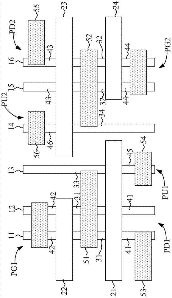
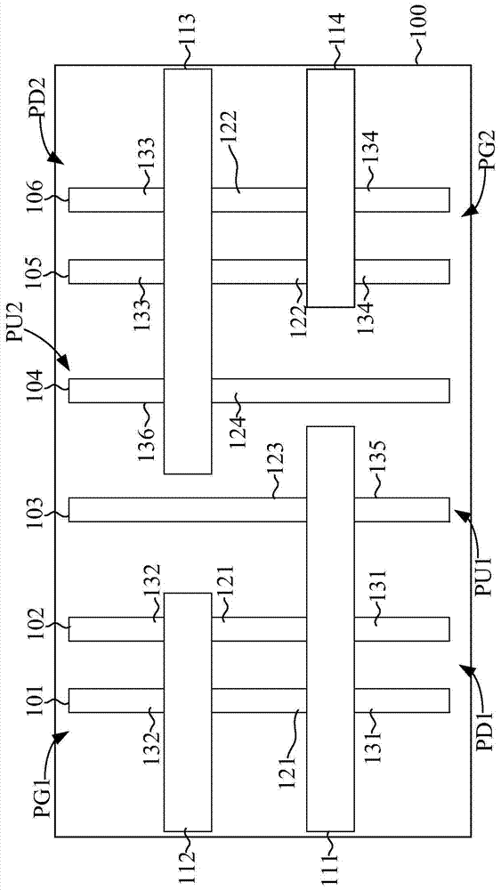
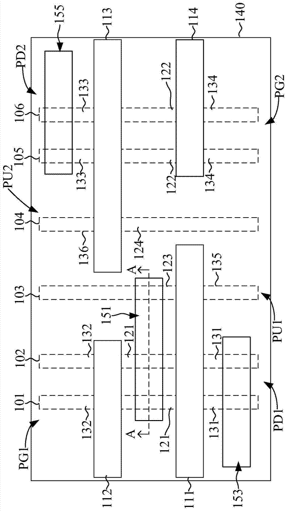
[0059] Aiming at the problems existing in the prior art, it is found through analysis: refer to figure 1 , the first metal layer 51 and the second metal layer 52 are formed in the same patterning step. Specifically, the method for forming the first metal layer 51 and the second metal layer 52 includes: first, forming a photoresist layer on the interlayer dielectric layer;

[0060] Expose the photoresist layer. During the exposure process, the bright area of ​​the mask corresponds to the position of the first metal layer and the second metal layer, and the photoresist layer corresponding to the bright area is exposed; then developing, the exposed photoresist layer partially removed;

[0061] Next, the patterned photoresist layer is used as a mask to etch the interlayer dielectric layer with a partial thickness to form the first groove and the second groove, and then the patterned photoresist layer is removed. Thereafter, a first metal layer is formed in the first trench and a...


PUM


Abstract

A method for forming an SRAM unit, comprising: forming: first, second, third, fourth, fifth, and sixth fins; a first grid across the first, second, and third fins; across the first, second The second gate of the fin, the first and second fins between the first and second gates are the first drain; the third gate across the fourth, fifth and sixth fins is across the fifth, The fourth gate of six fins, the fifth and sixth fins between the third and fourth gates are the second drain; the fifth source and third drain of the third fins on both sides of the first gate ; the sixth source and the fourth drain of the fourth fin on both sides of the third gate; forming an interlayer dielectric layer; the first patterning forms a first trench, across the first and second fins of the first drain part, the third fin of the third drain; the second patterning forms a second trench, across the fifth and sixth fins of the second drain, and the fourth fin of the fourth drain; in the first trench The groove forms the first metal layer, and the second groove forms the second metal layer. SRAM cells are realized technologically.

Description

technical field [0001] The invention relates to the technical field of semiconductors, in particular to a method for forming an SRAM unit. Background technique [0002] Static Random Access Memory (SRAM), as a member of memory, has the advantages of high speed, low power consumption and compatibility with standard processes, and is widely used in PCs, personal communications, consumer electronics (smart cards, digital cameras, Multimedia player) and other fields. [0003] A static random access memory includes a plurality of static random access memory units (hereinafter referred to as SRAM units), the plurality of SRAM units are arranged in an array, and a SRAM unit includes six transistors (6-T). As the integration level of integrated circuits increases, the feature size of SRAM cells gradually decreases and the wafer area occupied by them becomes smaller and smaller. Compared with the size of the planar MOS transistor, the size of the fin field effect transistor is smal...

Claims


Application Information

Patent Timeline
Patent Type & Authority Patents(China)
IPC IPC(8): H01L21/8244
CPCH10B10/00H10B10/12
Inventor 张弓傅丰华
Owner SEMICON MFG INT (SHANGHAI) CORP
Why Eureka
Try Eureka