

A passivation anti-reflection film for high pid resistant single crystal battery and its preparation process
A passivation reduction and reflective film technology, applied in the field of solar cells, can solve the problems of PID attenuation and battery conversion efficiency reduction, and achieve the effects of increasing short-circuit current, reducing overall refractive index, and increasing anti-PID attenuation characteristics.
- Summary
- Abstract
- Description
- Claims
- Application Information
AI Technical Summary
Problems solved by technology
Method used
Image

Examples
Embodiment 1
[0023] 1) Pretreatment of the original silicon wafer, the pretreatment includes processes such as texturing, diffusion and etching in the battery process;
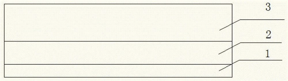
[0024] 2) Using high-voltage ionized or ultraviolet ionized oxygen to form a thin layer of dense SiO on the surface of the single crystal silicon wafer after etching x Layer 1, the refractive index is 1.65, and the film thickness is 0.8nm;
[0025] 3) Use PECVD equipment to coat the remaining film layer on the diffusion surface, cancel the pre-deposition step when coating the film, and coat SiO first x Layer 2, the refractive index is 1.65, and the film thickness is 2nm; then coat the top layer with a single layer of SiN x Layer 3, the refractive index is 2.05, and the film thickness is 75nm;
[0026] 4) Print the back electrode, aluminum back field, positive grid line and positive electrode using the traditional battery printing process, and sinter;
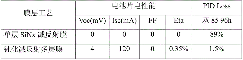
[0027] After testing, it is found that the photoelectric conversion ...
Embodiment 2
[0032] 1) Pretreatment of the original silicon wafer, the pretreatment includes processes such as texturing, diffusion and etching in the battery process;
[0033] 2) Using high-voltage ionized or ultraviolet ionized oxygen to form a thin layer of dense SiOx layer 1 on the surface of the monocrystalline silicon wafer after etching, the refractive index is 1.65, and the film thickness is 0.8nm;
[0034] 3) Use PECVD equipment to coat the remaining film layer on the diffusion surface, cancel the pre-deposition step during coating, and first coat SiOx layer 2 with a refractive index of 1.65 and a film thickness of 20nm; the top layer is a double-layer SiNx layer 3, and the bottom layer SiN has a refractive index 2.15, the film thickness is 20nm, the upper SiN refractive index is 2.05, and the film thickness is 35nm;
[0035] 4) Print the back electrode, aluminum back field, positive grid line and positive electrode using the traditional battery printing process, and sinter;
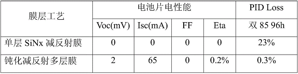
[0...
PUM
 Abstract
Description
Claims
Application Information