Electrode structure on back of solar cell and manufacturing method thereof

A technology of solar cells and back electrodes, applied in the field of solar cells, can solve the problems of expensive processing technology, reduce production costs, disadvantages, etc., and achieve the effects of improving conversion efficiency, reducing surface recombination rate, and improving infrared spectral response

Active Publication Date: 2012-09-19
陕西众森电能科技有限公司
View PDF3 Cites 5 Cited by
  • Summary
  • Abstract
  • Description
  • Claims
  • Application Information

AI Technical Summary

Problems solved by technology

However, the vacuum and laser used in the above process are relatively expensive processing technology, which is not conducive to reducing production costs

Method used


Image

  • Electrode structure on back of solar cell and manufacturing method thereof
  • Electrode structure on back of solar cell and manufacturing method thereof
  • Electrode structure on back of solar cell and manufacturing method thereof

Examples


Embodiment 1

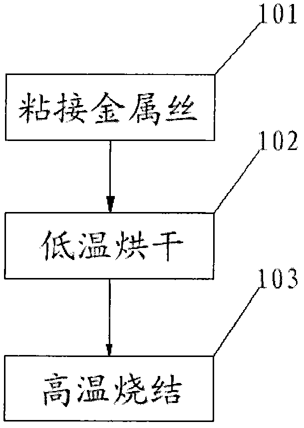
[0035] figure 1 It is a schematic flowchart of a method for fabricating a back electrode of a solar cell provided in Embodiment 1 of the present invention. see figure 1 As shown, the method mainly includes the following steps:

[0036] Step 101: bonding wires;

[0037] Stick the metal wire with conductive paste and paste it on the surface of the silicon wafer to form an electrode line;

[0038] Step 102: drying at low temperature;

[0039] Dry the silicon wafer bonded with the wire at a temperature of 200°C to 400°C;

[0040] Step 101: high temperature sintering;

[0041] The dried silicon wafer is sintered at a temperature of 500°C to 900°C. At the same time, the silicon wafer and the back electrode are sintered together to form a good ohmic contact between the conductive paste and the silicon wafer. At the same time, the The conductive paste is sintered with the wire to form a complete conductor.

[0042] Ohmic contact refers to the resistive contact between metal and...

Embodiment 2

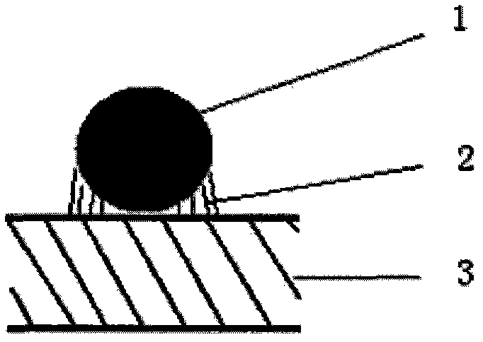
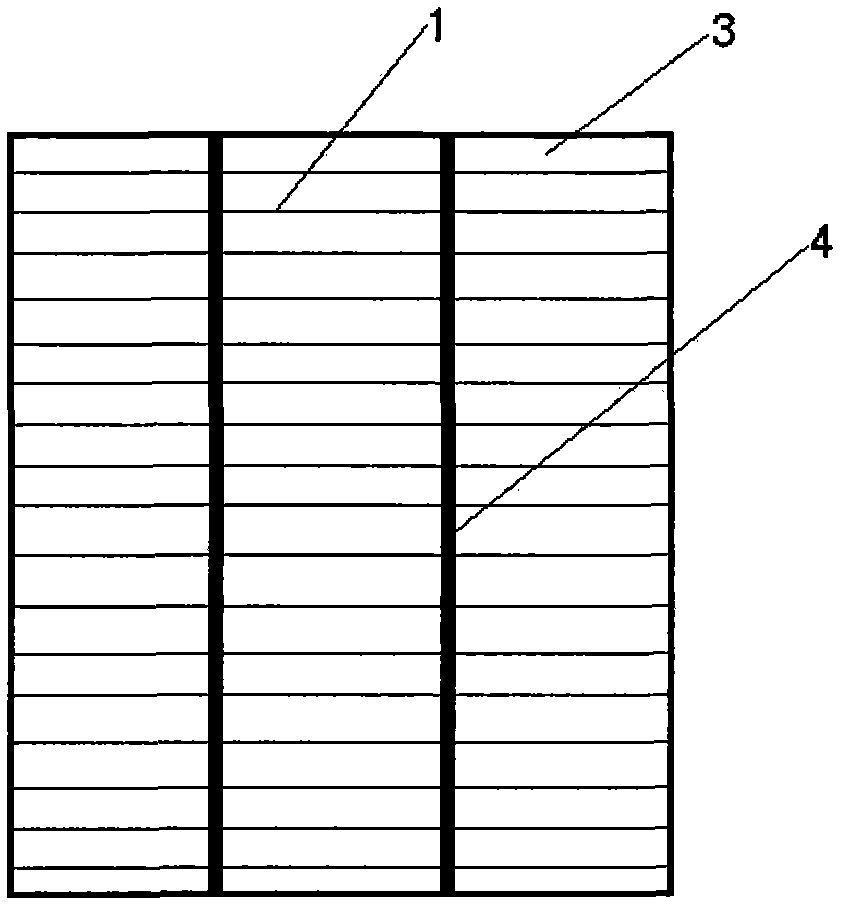
[0045] image 3 A schematic diagram of the back electrode structure of a solar cell provided by Embodiment 2 of the present invention; figure 2 It is a partial cross-sectional schematic diagram of a back electrode structure of a solar cell according to the present invention.

[0046] Such as figure 2 As shown, it includes a silicon chip 3 and a metal wire 1, the silicon chip 3 and the metal wire 1 are bonded together by a conductive paste 2, and the diameter of the metal wire 1 is 0.01 mm to 0.15 mm.

[0047] Such as image 3 As shown, the metal wires 1 are equally spaced and parallel bonded on the upper surface of the silicon wafer, and the distance between the metal wires is 0.5 to 3 mm.

[0048] Such as image 3 As shown, on the back surface of the silicon wafer 3, a busbar line is arranged perpendicular to the direction of the metal wire to lead out the back electrode. The busbar line corresponds to the front busbar line one by one, and the position is the same. 1 t...

Embodiment 3

[0052] Figure 4 A schematic diagram of the front electrode structure of a solar cell provided by Embodiment 3 of the present invention; figure 2 It is a partial cross-sectional schematic diagram of a front electrode structure of a solar cell according to the present invention.

[0053] Such as figure 2 As shown, it includes a silicon chip 3 and a metal wire 1, the silicon chip 3 and the metal wire 1 are bonded together by a conductive paste 2, and the diameter of the metal wire 1 is 0.01 mm to 0.15 mm.

[0054] Such as Figure 4 As shown, the metal wires 1 are equally spaced and parallel bonded on the upper surface of the silicon wafer, and the distance between the metal wires is 0.5 to 3 mm.

[0055] Such as Figure 4 As shown, one end of the metal wire 1 is provided with an electrode lead-out segment 5, and the electrode lead-out segment 5 protrudes from the surface of the silicon wafer 3 to lead out the back electrode.

[0056] When making this embodiment, first sti...


PUM


Abstract

The invention relates to the field of solar cells and particularly discloses an electrode structure on the back of a solar cell and a manufacturing method thereof. The electrode structure comprises a silicon chip and a metal wire which are adhered through electrocondution slurry, and the electrocondution slurry and the metal wire are formed into an integrated conductor through the steps of drying and sintering. According to the electrode structure on the back of the solar cell and the manufacturing method, an electrode or a point electrode, which is formed by the metal wire, can replace a face electrode on an original silicon chip. A good passivating layer and a reflecting layer can be manufactured in a non-electrode area, the surface recombination speed can be reduced by the good passivating, the infrared spectral response can be improved by the good reflection, and accordingly the conversion efficiency of the solar cell is improved.

Description

technical field [0001] The invention relates to the field of solar cells, in particular to a solar cell back electrode structure and a manufacturing method thereof. Background technique [0002] Crystalline silicon solar cells are the mainstream solar cells at present. The production process is as follows: de-damaging layer texture, diffusion, phosphorus-silicon glass removal, peripheral etching, PECVD deposition of silicon nitride passivation anti-reflection film, screen printing front and back Electrodes, front and back electrodes are co-sintered. Among them, screen printing is currently the main electrode production method. For P-type silicon wafers, printing aluminum paste and silver-aluminum paste are sintered to form the back surface electrode. As an improved process, an insulating passivation layer is first made on the entire back surface, and then vacuum evaporation The aluminum layer is then burned through the insulating layer with a laser at a certain interval, so...

Claims


Application Information

Patent Timeline
Patent Type & Authority Applications(China)
IPC IPC(8): H01L31/18H01L31/0224
CPCY02P70/50
Inventor 黄国保
Owner 陕西众森电能科技有限公司
Why Eureka
Try Eureka