Etching-technology-based silicon science (SIS) junction solar cell

A solar cell and technology technology, applied in circuits, photovoltaic power generation, electrical components, etc., can solve the problems of low conversion efficiency of SIS junction solar cells, and achieve the effects of reducing surface recombination rate, balancing photocurrent, and improving extraction efficiency

Inactive Publication Date: 2011-08-24
INST OF SEMICONDUCTORS - CHINESE ACAD OF SCI
View PDF3 Cites 5 Cited by
  • Summary
  • Abstract
  • Description
  • Claims
  • Application Information

AI Technical Summary

Problems solved by technology

[0007] In view of this, the main purpose of the present invention is to provide a SIS junction solar cell based on etching technology to solve the problem of low conversion efficiency of the current SIS junction solar cell and achieve the purpose of improving the optical absorption and carrier extraction capabilities of the cell

Method used


Image

  • Etching-technology-based silicon science (SIS) junction solar cell
  • Etching-technology-based silicon science (SIS) junction solar cell
  • Etching-technology-based silicon science (SIS) junction solar cell

Examples


Embodiment

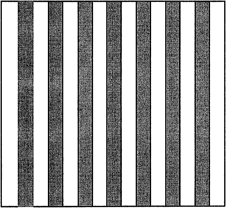
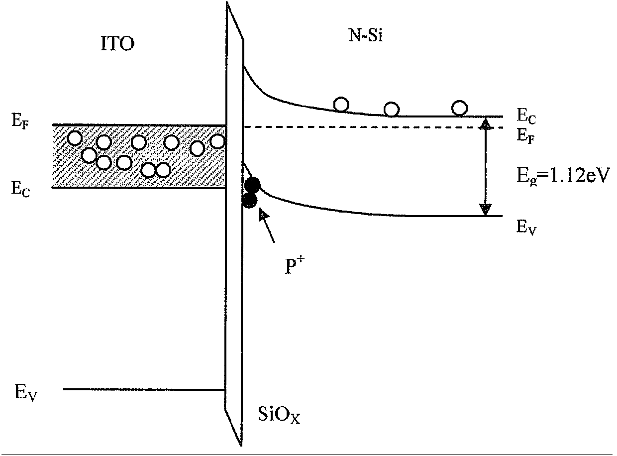
[0040] In this embodiment, the lower electrode 10 is Ti / Au. In order to improve the carrier collection efficiency and realize the ideal ohmic contact between the electrode and the light-absorbing material layer 20, the surface in contact with the lower electrode 10 needs to be heavily doped; optical absorption The material layer 20 is N-type single crystal Si with a band gap of 1.12eV and a thickness of 100 microns. The surface etching structure is a one-dimensional strip type, which is realized by photolithography and ICP etching. The specific parameters can be selected as a strip width of 10 microns , the period is 20 microns, the etching depth is 50 microns; the oxide insulating layer 30 passes through the H 2 o 2 Formed by corrosion, the thickness is about ten angstroms. The insulating layer can effectively reduce surface defects and improve the Schottky barrier; the TCO thin film layer 40 is selected as ITO, with a thickness of about 80nm, and is deposited on the oxide in...


PUM


Abstract

The invention discloses an etching-technology-based silicon science (SIS) junction solar cell, which comprises a lower electrode (10), a light absorption material layer (20), an oxide insulating layer (30), a total cost of ownership (TCO) thin-film layer (40), an upper pattern electrode (50) and nanoparticles (60), wherein the light absorption material layer (20) is prepared on the lower electrode (10); due to the etching technology, a micron-scale one-dimensional bar structure or two-dimensional columnar structure which has different periods and depths is prepared on the light absorption material layer (20); the oxide insulating layer (30) is formed by oxidizing the light absorption material layer (20) through a chemical method; the TCO thin-film layer (40) is deposited on the oxide insulating layer (30); the upper pattern electrode (50) is prepared on the TCO thin-film layer (40); and the nanoparticles (60) are arranged on the TCO thin-film layer (40). The problem that the conventional SIS junction solar cell has low conversion efficiency is solved, and the aim of improving the capacities of optical absorption of the cell and carrier extraction is fulfilled.

Description

technical field [0001] The invention relates to the technical field of semiconductor photovoltaic devices, in particular to an SIS (semiconductor-insulator-semiconductor) junction solar cell based on etching technology. Background technique [0002] Solar cells can directly convert sunlight energy into electrical energy and solve the current energy crisis facing the world. Therefore, the construction of low-cost, high-efficiency solar cells has become the focus of research in the photovoltaic industry at home and abroad. At present, semiconductor solar cells with single or multiple PN junction structures have been widely used in technical fields such as aerospace, military affairs, satellites, landscape lighting and household electricity. [0003] Solar cells take advantage of the photovoltaic effect of materials, the phenomenon in which a device generates a voltage when exposed to light. Currently commonly used solar cells are mostly made of semiconductor materials, using ...

Claims


Application Information

Patent Timeline
Patent Type & Authority Applications(China)
IPC IPC(8): H01L31/06H01L31/0352H01L31/0216
CPCY02E10/50
Inventor 马绍栋付非亚王宇飞王海玲彭红玲郑婉华
Owner INST OF SEMICONDUCTORS - CHINESE ACAD OF SCI
Why Eureka
Try Eureka