A method to enhance the optical absorption of cdin2s4

A technology of optical absorption and cdin2s4, which is applied in the field of semiconductor optoelectronic materials, can solve the problems of unfavorable carrier separation, disconnection, and affecting the photoelectric conversion performance of semiconductors, and achieve the goal of enhancing optical absorption capacity, enhancing optical absorption capacity, and improving photoelectric conversion efficiency. Effect

Active Publication Date: 2019-05-21
SHANGHAI DIANJI UNIV
View PDF4 Cites 0 Cited by
  • Summary
  • Abstract
  • Description
  • Claims
  • Application Information

AI Technical Summary

Problems solved by technology

[0004] In summary, in the prior art to CdIn 2 S 4 The improvement methods of optical absorption mainly focus on transition metal doping, and most of them stay in theoretical research, which is seriously out of touch with experiments; in addition, transition metal d electrons are too localized, which is not conducive to carrier separation, and it is easy to form new doping defects Recombination centers, which affect the actual photoelectric conversion performance of semiconductors

Method used


Image

  • A method to enhance the optical absorption of cdin2s4
  • A method to enhance the optical absorption of cdin2s4
  • A method to enhance the optical absorption of cdin2s4

Examples


Embodiment 1

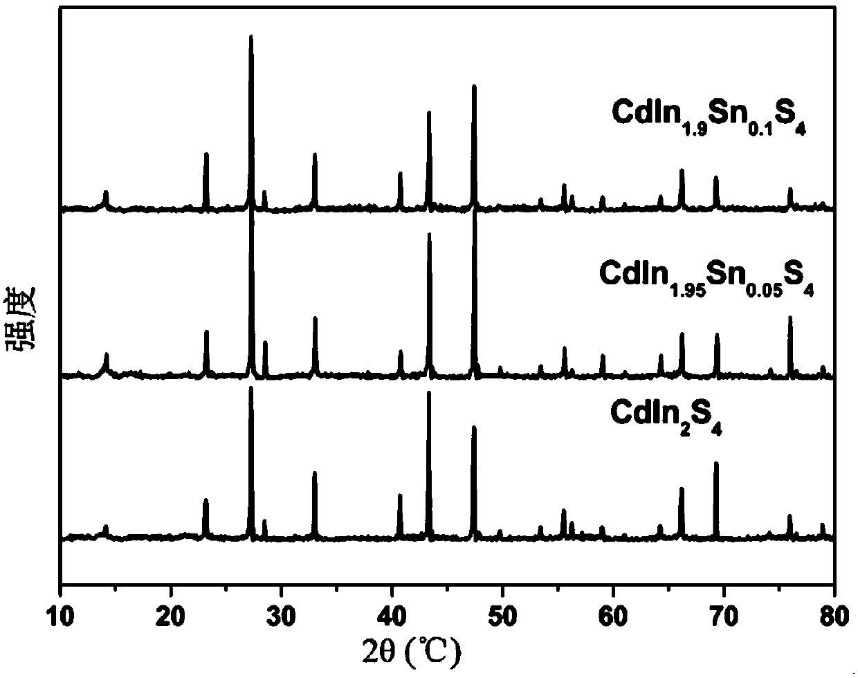
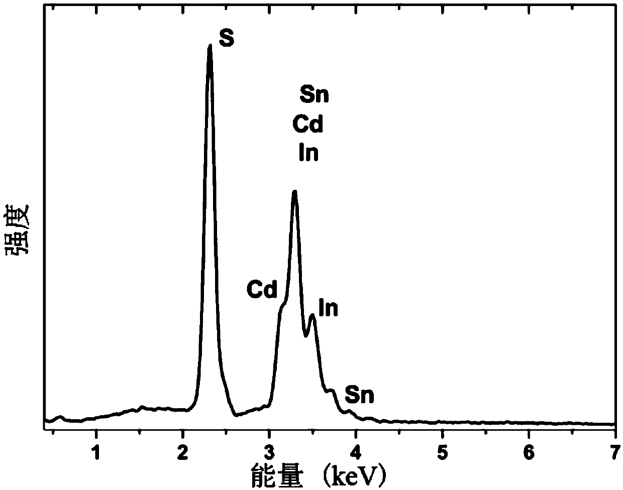
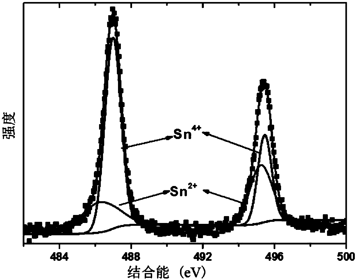
[0031] Example 1CdIn 2-x sn x S 4 (x=0,0.05,0.1) Preparation of materials

[0032] Cd powder (purity: 99.99%), In particles (purity: 99.999%), S powder (purity: 99.999%) and Sn powder (purity: 99.99%) according to CdIn 2-x sn x S 4Weigh the stoichiometric ratio of (x=0,0.05,0.1), put it into a quartz glass tube, and seal the quartz glass tube with a hydrogen-oxygen flame; put the fused quartz glass tube into a programmable temperature-controlled muffle furnace , slowly heated up to 750°C at a rate of 2°C / min and held for 24 hours, then cooled to room temperature with the furnace; after opening the tube again, the obtained sample was ground in an agate mortar, vacuum-packed in a quartz glass tube, and placed in a program control In a warm muffle furnace, slowly raise the temperature to 750°C at a rate of 2°C / min and then sinter and hold for 48 hours. The sample is cooled to room temperature with the furnace, and then ground again after opening the tube.

Embodiment 2

[0033] Example 2CdIn 2-x sn x S 4 (x=0,0.05,0.1) Preparation of materials

[0034] Binary compounds of Cd, In, S and Sn with a purity of not less than 99.99% are classified as CdIn 2-x sn x S 4 (x=0,0.05,0.1) stoichiometric ratio weighing, put into a quartz glass tube, and seal the quartz glass tube with a hydrogen-oxygen flame; put the fused quartz glass tube into a programmed temperature control muffle furnace , slowly heated up to 700°C at a rate of 5°C / min and held for 48 hours, then cooled to room temperature with the furnace; after opening the tube again, the obtained sample was ground in an agate mortar, vacuum-packed in a quartz glass tube, and controlled by the program In a warm muffle furnace, the temperature was slowly raised to 700°C at a rate of 5°C / min and then sintered and held for 24 hours. The sample was cooled to room temperature with the furnace, and then ground again after opening the tube.

Embodiment 3

[0035] Example 3CdIn 2-x sn x S 4 (x=0,0.05,0.1) Preparation of materials

[0036] Cd powder (purity: 99.99%), In particles (purity: 99.999%), S powder (purity: 99.999%) and Sn powder (purity: 99.99%) according to CdIn 2-x sn x S 4 Weigh the stoichiometric ratio of (x=0,0.05,0.1), put it into a quartz glass tube, and seal the quartz glass tube with a hydrogen-oxygen flame; put the fused quartz glass tube into a programmable temperature-controlled muffle furnace , slowly heated up to 750°C at a rate of 3°C / min and held for 24 hours, then cooled to room temperature with the furnace; after opening the tube again, the obtained sample was ground in an agate mortar, vacuum-packed in a quartz glass tube, and controlled by the program In a warm muffle furnace, the temperature was slowly raised to 800°C at a rate of 3°C / min and then sintered and held for 24 hours. The sample was cooled to room temperature with the furnace, and then ground again after opening the tube.


PUM


Abstract

The invention discloses a method for enhancing optical absorption of CdIn<2>S<4>. Specifically, a non-transition metal atom Sn is doped into CdIn<2>S<4> of a semiconductor, and a bandgap of the CdIn<2>S<4> is induced to generate an intermediate impurity band to generate a new optical absorption pathway, thereby achieving the target of enhancing optical absorption of the CdIn<2>S<4>. The method specifically comprises the steps of weighing raw materials of Cd, In, S and Sn according to a stoichiometric ratio of CdIn<2-x>Sn<x>S<4>; packaging the raw materials into a quartz glass tube in vacuum, heating the raw materials to 700-800 DEG C for reaction sintering; carrying out heat preservation for 24-48h and then carrying out furnace cooling; and carrying out secondary reaction sintering. According to the method, the optical absorption capability of the CdIn<2>S<4> is enhanced; and the method has a broad application prospect in the fields of photocatalysis and a photovoltaic cell.

Description

technical field [0001] The invention belongs to the technical field of semiconductor optoelectronic materials, in particular to an enhanced CdIn 2 S 4 The method of optical absorption. Background technique [0002] As a renewable and clean energy, solar energy has the advantages of abundant resources and no geographical restrictions. Using the photoelectric conversion effect of semiconductors can directly convert light into electricity, which is an important way for people to use solar energy. General semiconductor materials can only absorb photons whose energy is near the band gap, and photons whose energy is less than or beyond the band gap cannot be directly used by the semiconductor, resulting in energy loss. Through semiconductor doping technology, intermediate energy levels or energy bands are introduced into the semiconductor band gap, which can realize multiple absorption of sunlight, so as to make better use of solar spectrum energy. The theoretical limit efficie...

Claims


Application Information

Patent Timeline
Patent Type & Authority Patents(China)
IPC IPC(8): H01L31/18H01L31/032
CPCH01L31/0321H01L31/18Y02P70/50
Inventor 陈平张华马学亮王永存
Owner SHANGHAI DIANJI UNIV
Why Eureka
Try Eureka