A method for detecting the quality of the inner wall of a pcb via hole

A detection method and quality technology, applied in measuring devices, material analysis through optical means, image data processing, etc., can solve problems such as the inability to guarantee the quality of PCB products and the inability to detect the inner wall of the hole, so as to improve the stability of product performance, Guarantee product quality and realize the effect of improving profits

Active Publication Date: 2017-08-25
ZHEJIANG OULONG ELECTRIC
View PDF5 Cites 1 Cited by
  • Summary
  • Abstract
  • Description
  • Claims
  • Application Information

AI Technical Summary

Problems solved by technology

[0006] In order to overcome the shortcomings of the existing PCB detection methods that cannot detect the quality of the inner wall of the via hole and cannot guarantee the quality of the PCB product, the present invention provides a PCB via hole inner wall quality that can effectively detect the quality of the inner wall of the via hole and ensure the quality of the PCB product. detection method

Method used


Image

  • A method for detecting the quality of the inner wall of a pcb via hole
  • A method for detecting the quality of the inner wall of a pcb via hole
  • A method for detecting the quality of the inner wall of a pcb via hole

Examples


Embodiment Construction

[0051] The present invention will be further described below in conjunction with the accompanying drawings.

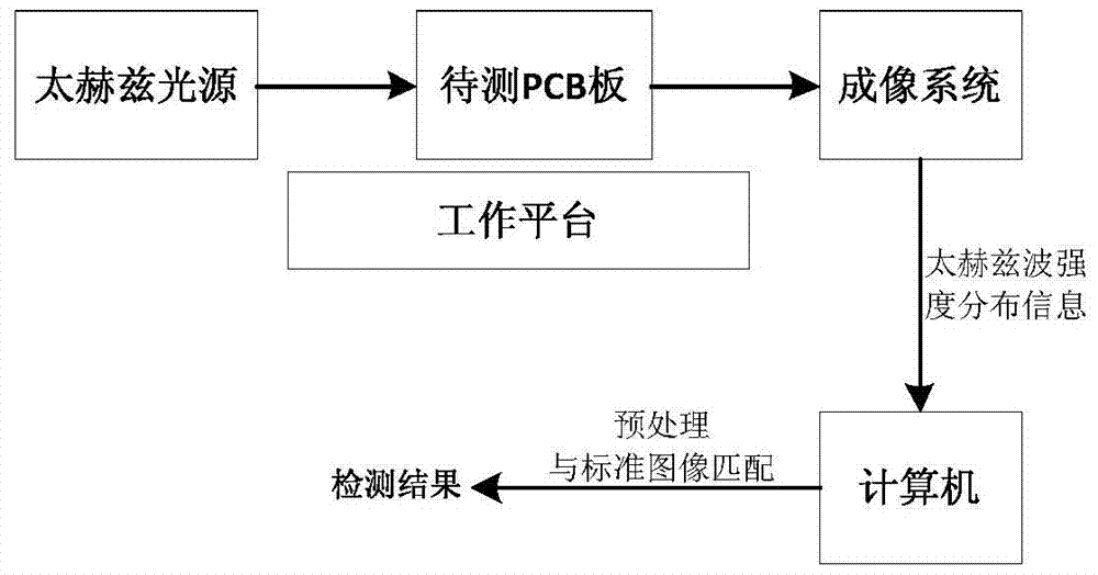
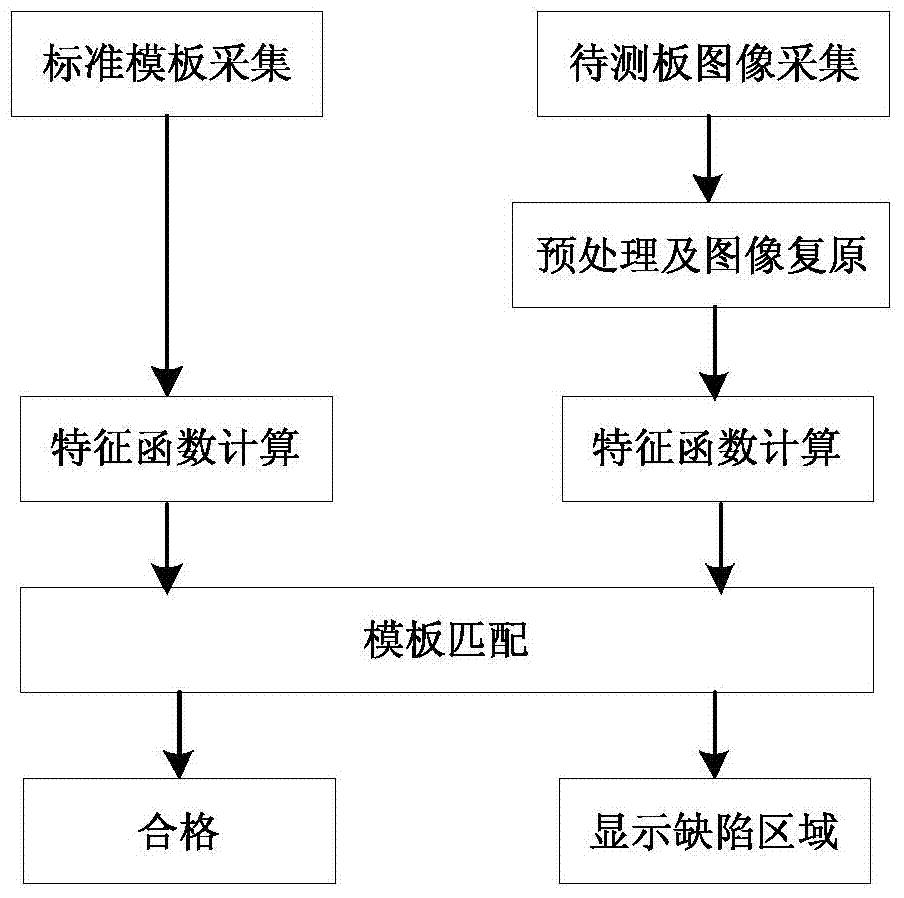
[0052] refer to Figure 1 ~ Figure 3 , a kind of detection method of PCB through-hole inner wall quality, described detection method comprises the steps:

[0053] Step 101: Obtain the PCB to be tested and a standard template;

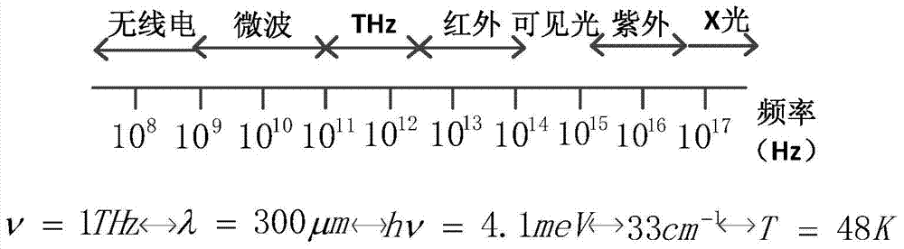
[0054] Step 102: Using terahertz wave imaging technology to collect the original image of the PCB to be tested and the original image of the standard template;

[0055] Step 103: Perform thresholding and denoising processing on the original image of the PCB to be tested and the original image of the standard template to obtain the restored image to be tested and the restored image of the standard template;

[0056] Step 104: Calculate the characteristic functions of the restored image of the standard template and the restored image to be tested respectively, and obtain the center and aperture information of the via hole. The process is as foll...


PUM


Abstract

A method for detecting the quality of the inner wall of a PCB via hole, comprising the following steps: Step 101: Obtain a PCB to be tested and a standard template; Step 102: Use terahertz wave imaging technology to collect the original image of the PCB to be tested and the original image of the standard template; Step 103: Perform thresholding and denoising processing on the original image of the PCB to be tested and the original image of the standard template to obtain the restored image to be tested and the restored image of the standard template; Step 104: Calculate the characteristic function of the restored image respectively, and obtain the via hole center and aperture information; Step 105 : Perform template matching operation on the feature information of the restored image of the standard template and the restored image to be tested; Step 106: If the matching operation result is within the allowable error range of production, then the detection is qualified; Step 107: If the result of the matching operation exceeds the allowable error range of production , it shows that the test failed. The invention effectively realizes the detection of the quality of the inner wall of the via hole and guarantees the quality of PCB products.

Description

technical field [0001] The invention relates to the field of detection methods for printed circuit boards (Printed Circuit Board, PCB), in particular to a detection method for the quality of the inner wall of a PCB via hole. Background technique [0002] Printed Circuit Board (PCB), as a main platform carrying a variety of electronic components, is responsible for connecting electronic components and making them truly a complete functional module. As an indispensable basic component of any electronic product, it has had a huge impact on the electronics industry in the world today. With the rapid development of the electronic industry, people have higher and higher requirements for product quality and stable performance, so the detection method of PCB has become an urgent research topic. [0003] In the existing inspection technology of PCB production, flying probes or special molds are generally used to detect the conduction electrical characteristics of PCB, and automatic ...

Claims


Application Information

Patent Timeline
Patent Type & Authority Patents(China)
IPC IPC(8): G01N21/3581G06T7/00
Inventor 刘恺杨力帆
Owner ZHEJIANG OULONG ELECTRIC
Why Eureka
Try Eureka