Liquid crystal display panel and manufacture method and display device thereof

A technology of a liquid crystal display panel and a manufacturing method, which are applied in the directions of nonlinear optics, instruments, optics, etc., can solve the problems of reduced transmittance, light leakage of the liquid crystal display panel, etc.

Inactive Publication Date: 2015-07-08
BOE TECH GRP CO LTD +1
View PDF7 Cites 13 Cited by
  • Summary
  • Abstract
  • Description
  • Claims
  • Application Information

AI Technical Summary

Problems solved by technology

[0005] Embodiments of the present invention provide a liquid crystal display panel, a manufacturing method thereof, and a display device, which are used...

Method used


Image

  • Liquid crystal display panel and manufacture method and display device thereof
  • Liquid crystal display panel and manufacture method and display device thereof
  • Liquid crystal display panel and manufacture method and display device thereof

Examples


Embodiment 1

[0043] Embodiment 1: Liquid crystal display panel in twisted nematic (Twist Nematic, TN) mode

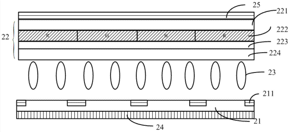
[0044] like figure 2 As shown, it is a schematic structural diagram of a liquid crystal display panel in TN mode provided by an embodiment of the present invention. The liquid crystal display panel mainly includes: an array substrate 21, a color filter substrate 22 arranged oppositely, and a The liquid crystal layer 23 between the color filter substrates 22, the first polarizer 24 arranged on the side of the array substrate 21 away from the color filter substrate 22, the first polarizer 24 arranged in the color filter substrate 22 away from the The second polarizer 25 on one side of the array substrate 21 , the first polarizer 24 is perpendicular to the polarization direction of the second polarizer 25 .

[0045] Wherein, the color filter substrate 22 involved in the embodiment of the present invention is arranged in sequence from far to near to the array substrate 21: a first bas...

Embodiment 2

[0067] Embodiment 2: LCD panel in ADS mode

[0068] like Image 6As shown, it is a schematic structural diagram of a liquid crystal display panel in TN mode provided by an embodiment of the present invention. The liquid crystal display panel mainly includes: an array substrate 61, a color filter substrate 62 arranged oppositely, and a The liquid crystal layer 63 between the color filter substrates 62 , the first polarizer 64 arranged on a side of the array substrate 61 away from the color filter substrate 62 , the first polarizer 64 arranged in the color filter substrate 62 away from the The second polarizer 65 on one side of the array substrate 61 , the first polarizer 64 is perpendicular to the polarization direction of the second polarizer 65 .

[0069] Wherein, the color filter substrate 62 involved in the embodiment of the present invention is arranged in sequence from far to near to the array substrate 61: a first transparent electrode 624, a first base 621, a color pho...

Embodiment 3

[0090] An embodiment of the present invention also provides a display device, including any one of the liquid crystal display panels mentioned above. Wherein, the display device may be any product or component with a display function such as a mobile phone, a tablet computer, a television, a monitor, a notebook computer, a digital photo frame, a navigator, and the like.


PUM


Abstract

The invention discloses a liquid crystal display panel and a manufacture method and a display device thereof. The manufacture method of the liquid crystal display panel mainly comprises the steps that through the canceling of a black matrix arranged at one side of a color film substrate, an insulation polarization layer is arranged at one side of an array substrate, and the polarization direction of the insulation polarization layer is perpendicular to the polarization direction of a first polarizing film at the side of the array substrate to be used for shielding leakage light generating by a gap between a data line and a public electrode wire. Due to the canceling of the black matrix, the uniformity of the surface of the color film substrate is guaranteed, and the probability of deviation generated by the alignment fitting is decreased; even if big deviation exits during the alignment fitting, the transmitted light of a pixel display area can not be shielded, and the transmittance of the pixel display area is guaranteed; in addition, the insulation polarization layer and the first polarizing film form a light shielding combination at the side of the array substrate to enable the leakage light generating by the gap of a wire running area to be shielded completely, and therefore the leakage of light caused by the deviation of the alignment fitting is avoided.

Description

technical field [0001] The invention relates to the field of display technology, in particular to a liquid crystal display panel, a manufacturing method thereof, and a display device. Background technique [0002] A traditional liquid crystal display panel includes a color filter substrate, an array substrate disposed opposite to each other, and a liquid crystal layer located between the color filter substrate and the array substrate. With the continuous update of technology and the continuous increase of demand, increasing the size of the glass substrate of the panel plays a vital role in improving production efficiency. [0003] However, as the size of the glass substrate increases, the difficulty of the manufacturing process increases. At the same time, the manufactured LCD panel also has serious quality defects. Among them, the biggest impact is that it is easy to reduce the alignment of the LCD panel. precision; moreover, there is a gap between the wiring area between ...

Claims


Application Information

Patent Timeline
IPC IPC(8): G02F1/1335
CPCG02F1/133528G02F1/1333
Inventor 刘晓那
Owner BOE TECH GRP CO LTD
Why Eureka
Try Eureka