Preparation method and positioning method for transmission electron microscope sample

A sample and lens technology, applied in the field of transmission electron microscope sample preparation, can solve problems such as poor judgment and inability to guarantee the success rate of sample preparation, and achieve the effect of simple positioning method, low cost, and accurate positioning

Active Publication Date: 2015-07-15
SHANGHAI HUALI MICROELECTRONICS CORP
View PDF8 Cites 28 Cited by
  • Summary
  • Abstract
  • Description
  • Claims
  • Application Information

AI Technical Summary

Problems solved by technology

In the above-mentioned method for preparing TEM samples using FIB technology, only the FIB Mark is made, and the FIB Mark is far away from the target position (such as figure 2 shown), it is difficult to judge, and the success rate of sample preparation cannot be guaranteed

Method used


Image

  • Preparation method and positioning method for transmission electron microscope sample
  • Preparation method and positioning method for transmission electron microscope sample
  • Preparation method and positioning method for transmission electron microscope sample

Examples


Embodiment Construction

[0034] In order to make the purpose and features of the present invention more obvious and understandable, the specific implementation of the present invention will be further described below in conjunction with the accompanying drawings. However, the present invention can be implemented in different forms and should not be limited to the described embodiments.

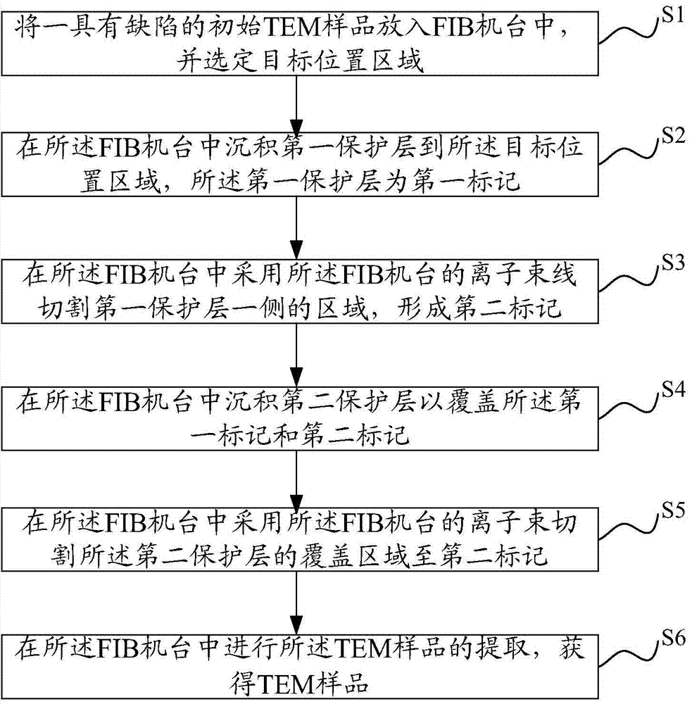
[0035] Please refer to image 3 , the present invention proposes a positioning method of a lens sample, comprising:

[0036] S1, put an initial TEM sample with defects into the FIB machine, and select the target location area;

[0037] S2. Depositing a first protective layer on the target position area in the FIB machine, where the first protective layer is a first mark;

[0038] S3, using the ion beam line of the FIB machine to cut an area on one side of the first protective layer in the FIB machine to form a second mark;

[0039] S4, depositing a second protective layer in the FIB machine to cover the first mark a...


PUM


Abstract

The invention provides a preparation method and positioning method for a transmission electron microscope sample. The preparation method comprises manufacturing two close marks, namely a first mark and a second mark, wherein the first mark is arranged at a target position region with a defect point, and the second mark is arranged according to the first mark position so that the second mark can be arranged at a position close to a target position. By virtue of the positioning method, the target position can be fast and accurately positioned according to the second mark so as to realize the precise positioning of a defect failure point; therefore, the preparation method and the position method provided by the invention are simple, low in cost, and capable of effectively realizing the precise positioning of the defect failure point and guaranteeing the success rate of the TEM sample preparation.

Description

technical field [0001] The invention relates to the field of semiconductor manufacturing, in particular to a preparation method and a positioning method of a transmission electron microscope sample. Background technique [0002] In the semiconductor production process, it is inevitable that there will be problems in the process of forming some semiconductor devices on the substrate, such as uneven film deposition thickness during the deposition process. Therefore, it is necessary to inspect the internal structure of the semiconductor device in real time during the production process to remove the problematic device or a part of the device and find out the cause of the problem, so as to facilitate subsequent production. [0003] The current commonly used method is to extract a sample that can be observed by a transmission electron microscope (TEM, Transmission electron microscope) from the substrate, and observe the cross-section of the TEM sample through the TEM to find the ...

Claims


Application Information

Patent Timeline
Patent Type & Authority Applications(China)
IPC IPC(8): G01N1/28
Inventor 高林史燕萍孙蓓瑶陈胜陈强
Owner SHANGHAI HUALI MICROELECTRONICS CORP
Why Eureka
Try Eureka