
Single photo avalanche diode imaging sensor for complementary metal oxide semiconductor stacked chip applications

An imaging sensor and semiconductor technology, applied in the field of imaging systems, can solve difficult problems such as relatively small-pitch photon timing sensors

Active Publication Date: 2015-07-15
OMNIVISION TECH INC
View PDF5 Cites 31 Cited by
  • Summary
  • Abstract
  • Description
  • Claims
  • Application Information

AI Technical Summary

Problems solved by technology

In addition, it is also difficult to realize relatively fine-pitch photonic timing sensors with high fill factor and superior SPAD performance in any single CMOS process

Method used


Image

  • Single photo avalanche diode imaging sensor for complementary metal oxide semiconductor stacked chip applications
  • Single photo avalanche diode imaging sensor for complementary metal oxide semiconductor stacked chip applications
  • Single photo avalanche diode imaging sensor for complementary metal oxide semiconductor stacked chip applications

Examples


Embodiment Construction

[0014] In the following description, numerous specific details are set forth in order to provide a thorough understanding of the present invention. It will be apparent, however, to one skilled in the art that the specific details need not be employed to practice the present invention. In other instances, well-known materials or methods have not been described in detail to avoid obscuring the present invention.

[0015] Reference throughout this specification to "one embodiment," "an embodiment," "an example," or "an example" means that a particular feature, structure, or characteristic described in connection with the embodiment or example includes In at least one embodiment of the invention. Thus, appearances of the phrases "in one embodiment," "in an embodiment," "an example," or "an example" in various places throughout this specification are not necessarily all referring to the same embodiment or example. Furthermore, particular features, structures or characteristics ma...


PUM


Abstract

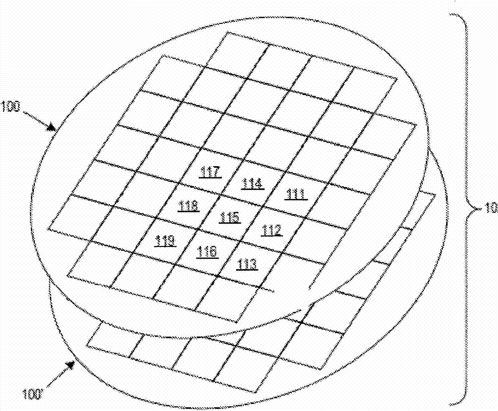
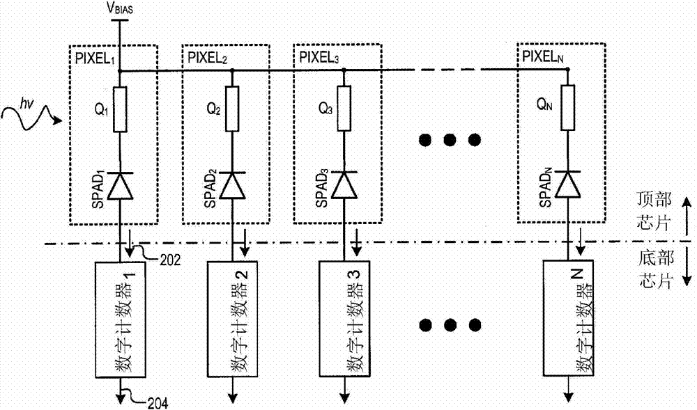
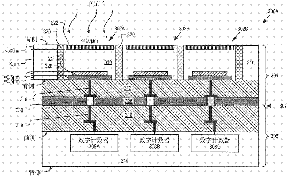
An imaging sensor system includes a single photon avalanche diode (SPAD) imaging array including N pixels formed in a first semiconductor layer of a first wafer. Substantially an entire thickness of the first semiconductor layer of each pixel is fully depleted such that a multiplication region included in each pixel near a front side is configured to be illuminated with photons through a back side and through the substantially entire thickness of the fully depleted first semiconductor layer. Deep n type isolation regions are disposed in the first semiconductor layer between the pixels to isolate the pixels. N digital counters are formed in a second semiconductor layer of a second wafer that is bonded to the first wafer. Each of the N digital counters is coupled to the SPAD imaging array and coupled to count output pulses generated by a respective one of the pixels.

Description

technical field [0001] The present invention relates generally to photodetectors, and more specifically, the present invention is directed to imaging systems that include single photon avalanche diode imaging sensors. Background technique [0002] Image sensors have become ubiquitous. It is widely used in digital still cameras, cellular phones, security cameras, as well as in medical, automotive and other applications. The technology used to manufacture image sensors has continued to advance rapidly. For example, demands for higher resolution and lower power consumption have driven further miniaturization and integration of these image sensors. [0003] One type of photodetector that can be used in an image sensor or in a photodetector is a single photon avalanche diode (SPAD). SPADs (also known as Geiger-mode avalanche photodiodes (GM-APDs)) are solid-state photodetectors capable of detecting low-intensity signals, eg, down to a single photon. A SPAD imaging sensor is a...

Claims


Application Information

Patent Timeline
IPC IPC(8): H01L27/146H04N5/374H04N5/3745
CPCH01L31/02027H01L31/107H01L27/14643H01L27/1463H01L27/14636H01L27/14609H01L27/14634
Inventor 埃里克·A·G·韦伯斯特
Owner OMNIVISION TECH INC
Learn More