OLED (organic light emitting display) device

A technology for display devices and pixels, applied in the field of OLED display devices, can solve the problems of deterioration of light-emitting properties of organic light-emitting layers, loss of electric field light-emitting properties, short-circuiting of electrodes, etc., to avoid short-circuiting of cathode and anode, improving display effect, and uniform thickness.

Active Publication Date: 2015-07-15
TCL CHINA STAR OPTOELECTRONICS TECH CO LTD
View PDF6 Cites 11 Cited by
  • Summary
  • Abstract
  • Description
  • Claims
  • Application Information

AI Technical Summary

Problems solved by technology

In the prior art, some pixel isolation layers are made of organic materials. It is found that when the pixel isolation layer of organic materials has an interface in contact with the organic light-emitting layer, moisture, oxygen, etc. in the pixel isolation layer will flow from the interface to the organic material. Diffusion of the light-emitting layer causes changes in the electronic state in the organic light-emitting layer, loses the ideal electric field luminescence characteristics, degrades the organic light-emitting layer, and affects the display effect
In order to improve the problems caused by the pixel isolation layer of organic materials, inorganic materials with low moisture and oxygen content have been used to make the pixel isolation layer. The substrate is erected at an angle close to 90 degrees, causing the thickness of the organic light-emitting layer and the common electrode at the position corresponding to the side wall to be significantly thinner than other positions, and even cause discontinuity, and moisture and oxygen will be significantly thinner or worse from the common electrode. The discontinuity enters the organic light-emitting layer, causing the light-emitting characteristics of the organic light-emitting layer to deteriorate. In addition, when the organic light-emitting layer has a discontinuity at the side wall, the distance between the common electrode and the pixel electrode may also be very close, resulting in a short circuit between the two electrodes. , causing damage to the organic light-emitting layer

Method used


Image

  • OLED (organic light emitting display) device
  • OLED (organic light emitting display) device
  • OLED (organic light emitting display) device

Examples


Embodiment Construction

[0028] In order to further illustrate the technical means adopted by the present invention and its effects, the following describes in detail in conjunction with preferred embodiments of the present invention and accompanying drawings.

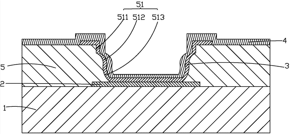
[0029] see figure 1 , the present invention provides an OLED display device, comprising:

[0030] Substrate 1;

[0031] A plurality of pixel areas arranged in an array on the substrate 1, each pixel area includes a pixel electrode 2, an organic light-emitting layer 3, and a common electrode 4 sequentially stacked on the substrate 1;

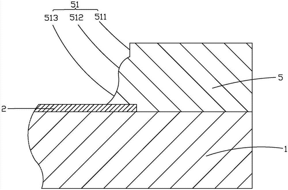
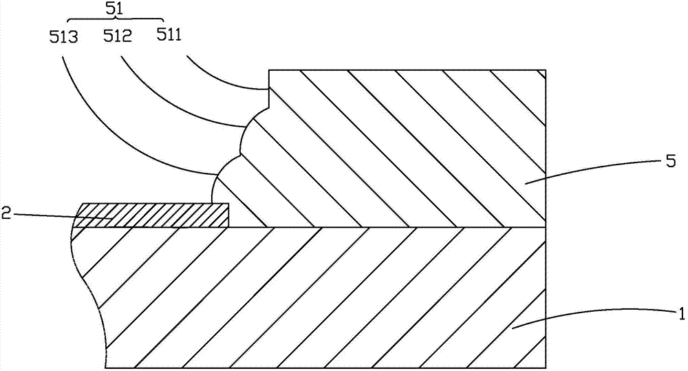
[0032] And a pixel isolation layer 5 with a plurality of openings, the pixel isolation layer 5 isolates each pixel area from other pixel areas, the openings are surrounded by side walls 51 of the pixel isolation layer, and each opening corresponds to a pixel area .

[0033] Wherein, the pixel electrode 2 and the organic light-emitting layer 3 are located in the opening, and the organic light-emitting layer 3 c...


PUM


Abstract

The invention provides an OLED (organic light emitting display) device. The OLED device comprises a substrate (1), a pixel electrode (2), an organic light-emitting layer (3), a common electrode (4) and a pixel isolation layer (5), wherein the pixel electrode (2), the organic light-emitting layer (3) and the common electrode (4) are sequentially stacked on the substrate (1) in each pixel region, the pixel isolation layer (5) is provided with multiple openings, the openings are defined by a side wall (51) of the pixel isolation layer (5) in a surrounding manner, and each opening corresponds to one pixel region; the pixel isolation layer (5) is made of an inorganic material, the side wall (51) of the pixel isolation layer comprises a straight line part (511), a first curve part (512) and a second curve part (513) which are arranged from top to bottom, the deterioration problem of the organic light-emitting layer (3) caused by the side wall (51) of the pixel isolation layer is solved, the organic light-emitting layer (3) and the common electrode (4) are prevented from being separated in the position of the side wall (51) of the pixel isolation layer, the common electrode (4) and the pixel electrode (2), namely, an anode and a cathode of the OLED device are prevented from short circuit, and the display effect is improved.

Description

technical field [0001] The invention relates to the field of display technology, in particular to an OLED display device. Background technique [0002] Organic Light Emitting Display (OLED) devices not only have excellent display performance, but also have the characteristics of self-luminescence, simple structure, ultra-thin, fast response, wide viewing angle, low power consumption and flexible display. , known as the "dream display", has been favored by major display manufacturers and has become the main force of the third-generation display devices in the field of display technology. [0003] OLED display devices are self-emissive display devices, usually including pixel electrodes used as anodes and cathodes, common electrodes, and an organic light-emitting layer arranged between the pixel electrodes and the common electrodes, so that when an appropriate voltage is applied to the anode When combined with a cathode, light is emitted from the organic light-emitting layer....

Claims


Application Information

Patent Timeline
Patent Type & Authority Applications(China)
IPC IPC(8): H01L27/32H01L51/52
CPCH10K59/122H10K59/1201
Inventor 吕晓文李文辉
Owner TCL CHINA STAR OPTOELECTRONICS TECH CO LTD
Why Eureka
Try Eureka