Unlock instant, AI-driven research and patent intelligence for your innovation.

Carrier, thin film transistor array substrate manufacturing method and liquid crystal display panel manufacturing method

A technology of thin film transistors and array substrates, which is applied in the field of liquid crystal displays, can solve the problems of reducing the production yield of thin film transistor array substrates and liquid crystal panels, deformation, and warping of ultra-thin glass substrates, so as to achieve difficult support, protect the environment, and improve production The effect of yield

Inactive Publication Date: 2015-07-22
HONG FU JIN PRECISION IND (SHENZHEN) CO LTD +1
View PDF6 Cites 4 Cited by
  • Summary
  • Abstract
  • Description
  • Claims
  • Application Information

AI Technical Summary

Problems solved by technology

However, since the thickness of the ultra-thin glass substrate is usually between 0.02 mm and 0.2 mm, the ultra-thin glass substrate is prone to warping or deformation during the manufacturing process of the thin film transistor array and pixel electrodes, thereby reducing the thickness of the thin film transistor array substrate. and LCD panel production yield

Method used


Image

  • Carrier, thin film transistor array substrate manufacturing method and liquid crystal display panel manufacturing method
  • Carrier, thin film transistor array substrate manufacturing method and liquid crystal display panel manufacturing method
  • Carrier, thin film transistor array substrate manufacturing method and liquid crystal display panel manufacturing method

Examples


Embodiment Construction

[0016] The embodiments of the present invention will be further described in detail below in conjunction with the accompanying drawings.

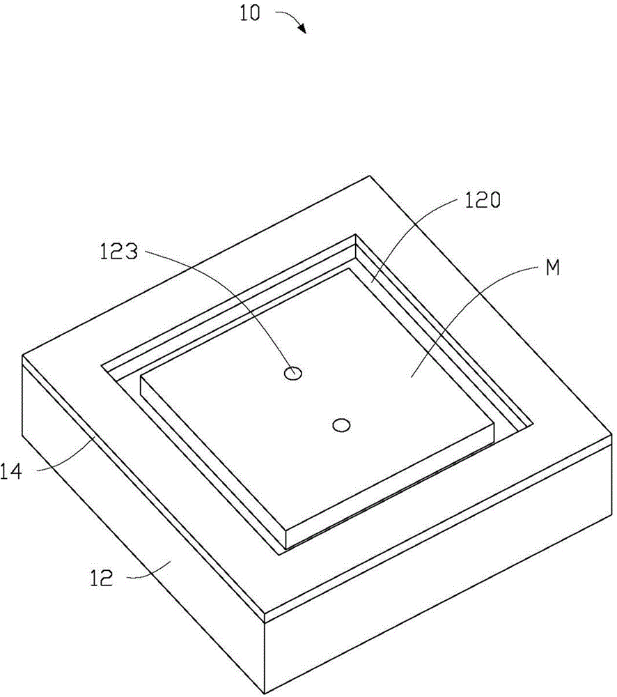
[0017] see figure 1 , is the carrier 10 provided in the first embodiment of the present invention. The carrier 10 includes a body 12 and an adhesive layer 14 .

[0018] Please combine figure 2 , the body 12 has a rectangular structure and includes a top surface 122 and a bottom surface 124 . The top surface 122 and the bottom surface 124 are respectively located on opposite sides of the main body 12 , and the top surface 122 is parallel to the bottom surface 124 . The top surface 122 defines a closed first groove 120 in the shape of a rectangular ring, and the first groove 120 does not penetrate through the bottom surface 124 . The area surrounded by the first groove 120 is defined as the active area M. The main body 12 defines a plurality of ventilation holes 123 passing through the top surface 122 and the bottom surface 124 , and th...


PUM

PropertyMeasurementUnit
Thicknessaaaaaaaaaa

Abstract

The invention relates to a carrier which comprises a carrier body and an adhesive layer. The carrier body comprises a top face and a bottom face which are opposite to each other, and a first groove which is in a closed mode and is shaped like a ring is formed in the top face; the adhesive layer is of a closed ring-shaped structure, the adhesive layer is arranged on the top face and surrounds the first groove, and glass powder is distributed in the adhesive layer. The invention further relates to a thin film transistor array substrate manufacturing method and a liquid crystal display panel manufacturing method.

Description

technical field [0001] The invention relates to the field of liquid crystal displays, in particular to a carrier, a method for manufacturing a thin film transistor array substrate using the carrier, and a method for manufacturing a liquid crystal panel using the carrier. Background technique [0002] The liquid crystal panel is formed by arranging liquid crystal molecules between the thin film transistor array substrate and the color filter substrate and encapsulating the cells. When manufacturing thin film transistor array substrates, thicker glass is used as the substrate, then thin film transistor arrays and pixel electrodes are manufactured on the substrate, and finally the substrate is chemically thinned to produce the currently popular ultra-thin thin film transistor arrays substrate. Because hydrofluoric acid (HF) is needed for chemical thinning, however, hydrofluoric acid is a strong acid, and if its waste liquid is not properly treated, it will cause irreparable im...

Claims


Application Information

Patent Timeline
IPC IPC(8): G02F1/13G02F1/1333
CPCG02F1/1303H01L27/1262
Inventor 张仁淙
Owner HONG FU JIN PRECISION IND (SHENZHEN) CO LTD
Features
  • R&D
  • Intellectual Property
  • Life Sciences
  • Materials
  • Tech Scout
  • Unparalleled Data Quality
  • Higher Quality Content
  • 60% Fewer Hallucinations
Learn More