A detection method for double masks in opc

A detection method and mask technology, which is applied in the field of semiconductors, can solve the problems of polysilicon pattern distortion, low accuracy of double pattern detection results, and failure to consider various influencing factors, etc., to achieve the effect of small running time

Active Publication Date: 2019-05-17
SEMICON MFG INT (SHANGHAI) CORP
View PDF4 Cites 0 Cited by
  • Summary
  • Abstract
  • Description
  • Claims
  • Application Information

AI Technical Summary

Problems solved by technology

[0007] Therefore, although there is a double-pattern monitoring method for polysilicon patterns in the prior art, the method is too simple and does not consider various influencing factors in the actual process, and the accuracy of the detection result for the double-pattern is low, resulting in the final The polysilicon pattern is distorted, and further improvements to existing methods are needed to eliminate the various problems existing in the prior art

Method used


Image

  • A detection method for double masks in opc
  • A detection method for double masks in opc
  • A detection method for double masks in opc

Examples


Embodiment 1

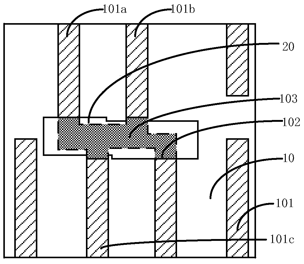
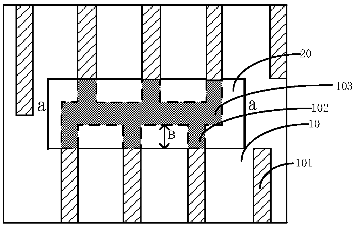
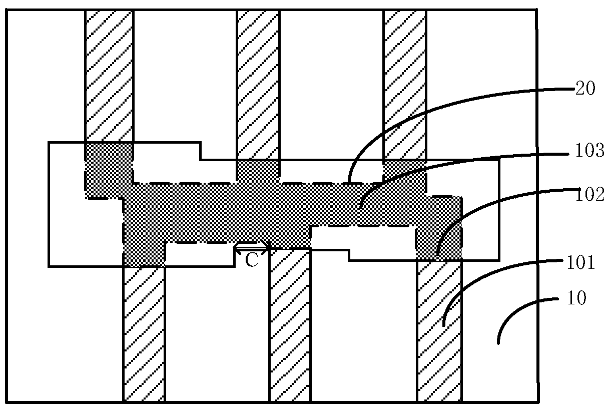
[0081] attached figure 2 It is the SEM picture of the mask in the process of mask pattern detection in a specific embodiment of the present invention, below in conjunction with the attached figure 2 A specific embodiment of the present invention will be further described.

[0082] exist figure 2 The left side of the middle is the SEM image of the pattern prepared in the actual process, and the right side is the structural schematic diagram. When the method of the prior art is selected for inspection, it can be seen from the figure on the right that the second mask plate 20 With a square hole, the second mask plate 20 can completely cover the pattern to be removed. Although there is a hole, it can still cover the scattering strip 30. Due to errors in alignment, in the actual process Due to the existence of alignment errors, the holes in the second mask 20 expose the scattering strips 30, which cannot be completely removed, and the defects shown in the left figure are forme...


PUM


Abstract

The present invention relates to a detection method for double masks in OPC. The detection method comprises: (a) providing a first mask and a second mask, and determining the pattern to be removed and the pattern to be finally retained in the first mask; (b) performing routine checking steps, such that it is ensured that the second mask encloses the pattern to be removed and does not contact the pattern to be finally retained; and (c) performing a process variable checking step, such that it is ensured that the alignment error and the etching error of the second mask are within the acceptable range. The detection method of the present invention has the following advantages that: the fidelity of the double masks in the target pattern can be ensured to the greatest degree; the influence of various variables during the process is considered, wherein the variables comprise litho overlay shift, etch bias variation and the like; and the influence on the OPC process and the operation time of the OPC lithography mask output is low.

Description

technical field [0001] The invention relates to the field of semiconductors, and in particular, the invention relates to a method for detecting double masks in OPC. Background technique [0002] Integrated circuit manufacturing technology is a complicated process, and the technology is updated very quickly. A key parameter that characterizes integrated circuit manufacturing technology is the minimum feature size, that is, critical dimension (CD). As the critical dimension shrinks, it even shrinks to the nanometer level, and it is precisely because of the reduction of the critical dimension that each It is possible to set millions of devices on a chip. [0003] Photolithography is the driving force behind the development of integrated circuit manufacturing processes, and it is also one of the most complex technologies. Compared with other single manufacturing technologies, the improvement of lithography technology is of great significance to the development of integrated ci...

Claims


Application Information

Patent Timeline
Patent Type & Authority Patents(China)
IPC IPC(8): G03F1/44G03F1/36
CPCG03F1/36G03F1/44
Inventor 王铁柱
Owner SEMICON MFG INT (SHANGHAI) CORP
Why Eureka
Try Eureka