Read-write control circuit and method for Flash chip and AMOLED (Active Matrix/Organic Light Emitting Diode) application circuit

A technology of read-write control and timing control circuit, which is applied in the field of AMOLED application circuit and read-write control circuit, and can solve problems such as abnormal display in the display area.

Active Publication Date: 2015-07-29
BOE TECH GRP CO LTD
View PDF5 Cites 7 Cited by
  • Summary
  • Abstract
  • Description
  • Claims
  • Application Information

AI Technical Summary

Problems solved by technology

In this way, the display of some display a

Method used


Image

  • Read-write control circuit and method for Flash chip and AMOLED (Active Matrix/Organic Light Emitting Diode) application circuit
  • Read-write control circuit and method for Flash chip and AMOLED (Active Matrix/Organic Light Emitting Diode) application circuit
  • Read-write control circuit and method for Flash chip and AMOLED (Active Matrix/Organic Light Emitting Diode) application circuit

Examples


Embodiment Construction

[0015] Various embodiments of the present invention will be described in detail below in conjunction with the accompanying drawings.

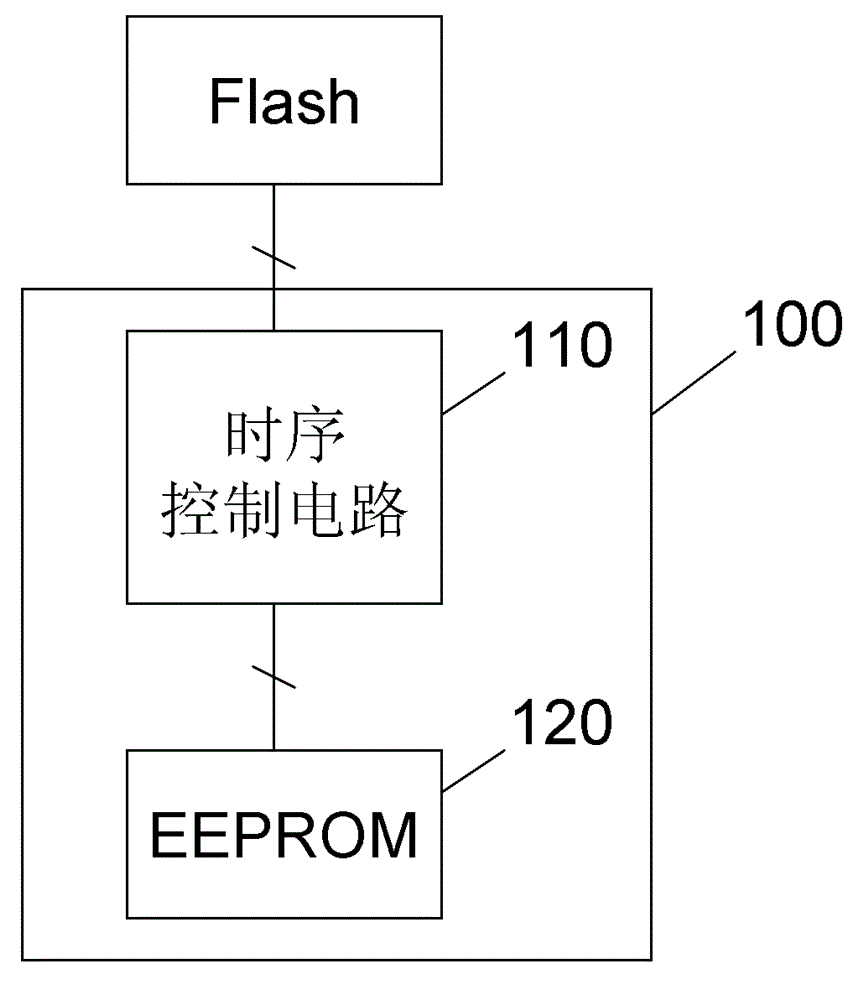
[0016] figure 1 A read / write control circuit 100 for a Flash chip according to an embodiment of the present invention is schematically illustrated. The read / write control circuit 100 includes a timing control circuit 110 and a first non-volatile memory 120 . exist figure 1 , the first non-volatile memory 120 is illustrated as an Electrically Erasable Programmable Read Only Memory (EEPROM).

[0017] The timing control circuit 110 generates read and write timing signals for the Flash chip. These read and write timing signals transmit control, address and data signals to the Flash chip through the I / O interface of the Flash chip, thereby performing operations such as programming (programming), erasing, and reading the Flash. It should be pointed out that although the interfaces of various products or manufacturers may be different, whether it ...


PUM


Abstract

The invention discloses a read-write control circuit for a Flash chip. The read-write control circuit for the Flash chip comprises a time sequence control circuit and a first non-volatile memory, wherein the time sequence control circuit generates a read-write time sequence signal for the Flash chip; the first non-volatile memory is used for storing multiple zone bits corresponding to multiple partitions in the Flash chip; each of zone bit indicates whether each corresponding partition is normally written in or not. The invention also discloses a read-write control method for the Flash chip, and an AMOLED (Active Matrix/Organic Light Emitting Diode) application circuit used for an electricity compensation mechanism and provided with the read-write control circuit. The zone bits are set to mark each partition, and a backup storage zone is set to retain original compensation data, so that the continuity of displaying and the completeness of electricity compensation data are ensured under the condition of power failure.

Description

technical field [0001] The invention relates to AMOLED module circuit technology, in particular to a read-write control circuit and method for a Flash chip. The present invention further relates to an AMOLED application circuit. Background technique [0002] In the conventional flat panel display circuit design, there are very few opportunities to write to the Flash chip. Generally, the data is written into the Flash chip when the product leaves the factory. When using it, it is only necessary to read the data in the chip without writing it. [0003] The current AMOLED module will be equipped with electrical compensation technology. Electrical compensation technology not only needs to write data to Flash when leaving the factory, but also needs to read and write to Flash during product use. However, during the user's use, abnormal events such as sudden power failure (for example, due to power failure or plug drop) may occur. At this time, if the Flash is in the writing s...

Claims


Application Information

Patent Timeline
IPC IPC(8): G11C16/06G11C16/26
CPCG11C16/16G06F3/0619G06F3/065G06F3/0688G06F12/00G11C5/141G11C5/148G11C16/10G11C16/20G11C16/26G11C16/32
Inventor 解红军
Owner BOE TECH GRP CO LTD
Why Eureka
Try Eureka