Supercharge Your Innovation With Domain-Expert AI Agents!

Semiconductor structure and layout structure of memory element

A memory element and layout structure technology, which is applied in the field of semiconductor structure and layout structure, can solve problems such as failure of flash memory memory elements and affecting element performance, and achieve the effect of improving reliability and increasing the tolerance of manufacturing process

Active Publication Date: 2015-07-29
UNITED MICROELECTRONICS CORP
View PDF4 Cites 3 Cited by
  • Summary
  • Abstract
  • Description
  • Claims
  • Application Information

AI Technical Summary

Problems solved by technology

As the tolerance (process window) of the device and the manufacturing process shrinks, the misalignment between the select gate and the contact plug will affect the performance of the device more and more, and even lead to the failure of the flash memory device.
In addition, when the selection gate is a spacer-type selection gate, it has an inclined and uneven surface, so the contact plug disposed on the selection gate and must be in physical contact with the selection gate is not easy to contact with the selection gate. Surfaces are actually in contact, which raises reliability issues

Method used


Image

  • Semiconductor structure and layout structure of memory element
  • Semiconductor structure and layout structure of memory element
  • Semiconductor structure and layout structure of memory element

Examples


Embodiment Construction

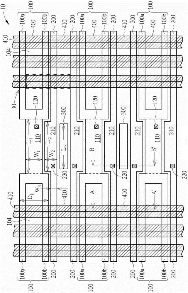
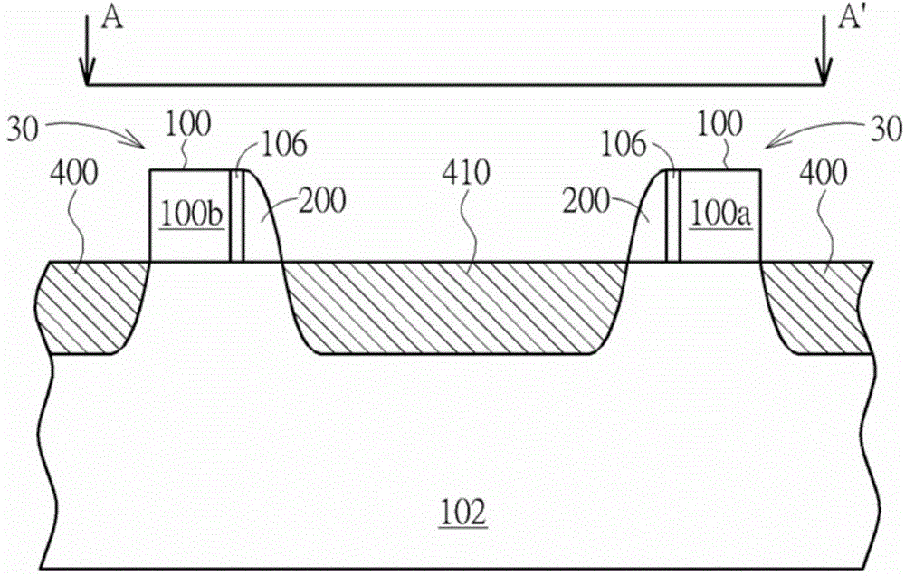
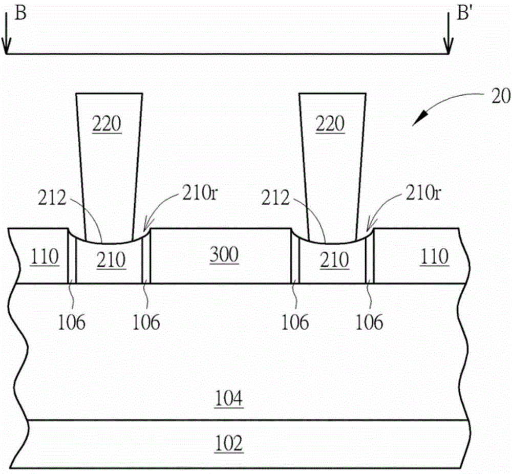
[0014] see Figure 1-3 ,in figure 1 A schematic diagram of a preferred embodiment of a layout structure of a memory element provided by the present invention, figure 2 for figure 1 A schematic cross-sectional view of the semiconductor structure of the memory element obtained along the A-A' tangent line, image 3 for figure 1 The schematic cross-sectional view of the semiconductor structure of the memory element obtained along the B-B' tangent line.

[0015] See first figure 1 . According to a preferred embodiment of the present invention, a layout structure 10 of a memory element includes a plurality of first gate patterns 100a, 100b serving as memory gates of the memory element. More importantly, the first gate patterns 100a, 100b of this preferred embodiment are as figure 1 Shown in pairs. That is to say, two parallel first gate patterns 100a, 100b form a first gate pattern pair (pair) 100, and the first gate patterns 100a, 100b in each first gate pattern pair 100 ...


PUM


Abstract

The invention discloses a semiconductor structure and a layout structure of a memory element. The layout structure of the memory element comprises a plurality of first gate patterns, a plurality of first contact pad patterns, a plurality of dummy patterns, a plurality of second contact pad patterns and a plurality of second gate patterns, wherein the first contact patterns are mutually parallel and electrically connected with the first gate patterns; the dummy patterns and the first contact patterns are arranged in a staggered mode, and each second contact pattern is arranged between on first contact pattern and one dummy pattern. In addition, the second gate patterns are electrically connected to the second contact patterns respectively.

Description

technical field [0001] The invention relates to a semiconductor structure and a layout structure of a memory element, in particular to a semiconductor structure and a layout structure of a flash memory element. Background technique [0002] Semiconductor memory devices are commonly used in various electronic devices. For example, non-volatile semiconductor memory (non-volatile semiconductor memory) is often used in mobile phones, digital cameras, personal digital assistants, mobile computing devices, non-mobile computing devices and other device. Among non-volatile semiconductor memories, Electrically Erasable Programmable Read Only Memory (EEPROM) and flash memory are the most widely used non-volatile semiconductor memories. memory. [0003] However, with the progress of the semiconductor manufacturing process and the shrinkage of the components, the semiconductor memory components are faced with more challenges. For example, a conventional flash memory cell includes a m...

Claims


Application Information

Patent Timeline
IPC IPC(8): H01L27/115H01L29/423
Inventor 陈震王献德邱意珊程伟
Owner UNITED MICROELECTRONICS CORP
Features
  • R&D
  • Intellectual Property
  • Life Sciences
  • Materials
  • Tech Scout
  • Unparalleled Data Quality
  • Higher Quality Content
  • 60% Fewer Hallucinations
Learn More