GOA circuit based on oxide semiconductor thin-film transistor

An oxide semiconductor and thin film transistor technology, applied in static memory, instruments, static indicators, etc., can solve the problems affecting the normal output of the GOA circuit, affecting the pull-down maintenance, abnormal screen display, etc., to eliminate interference, improve reliability, The effect of preventing electric leakage

Active Publication Date: 2015-08-19
SHENZHEN CHINA STAR OPTOELECTRONICS TECH CO LTD
View PDF5 Cites 34 Cited by
  • Summary
  • Abstract
  • Description
  • Claims
  • Application Information

AI Technical Summary

Problems solved by technology

However, there are still certain problems in the existing GOA circuit based on oxide semiconductor thin film transistors. For example, if N is a positive integer, in the Nth-level GOA unit circuit, since the first constant voltage negative potential VSS and the second The constant voltage negative potential DCL, the Nth stage GOA unit circuit has the problem of crosstalk current during the inactive period; since the drain of a thin film tra

Method used


Image

  • GOA circuit based on oxide semiconductor thin-film transistor
  • GOA circuit based on oxide semiconductor thin-film transistor
  • GOA circuit based on oxide semiconductor thin-film transistor

Examples


Embodiment Construction

[0043] In order to further illustrate the technical means adopted by the present invention and its effects, the following describes in detail in conjunction with preferred embodiments of the present invention and accompanying drawings.

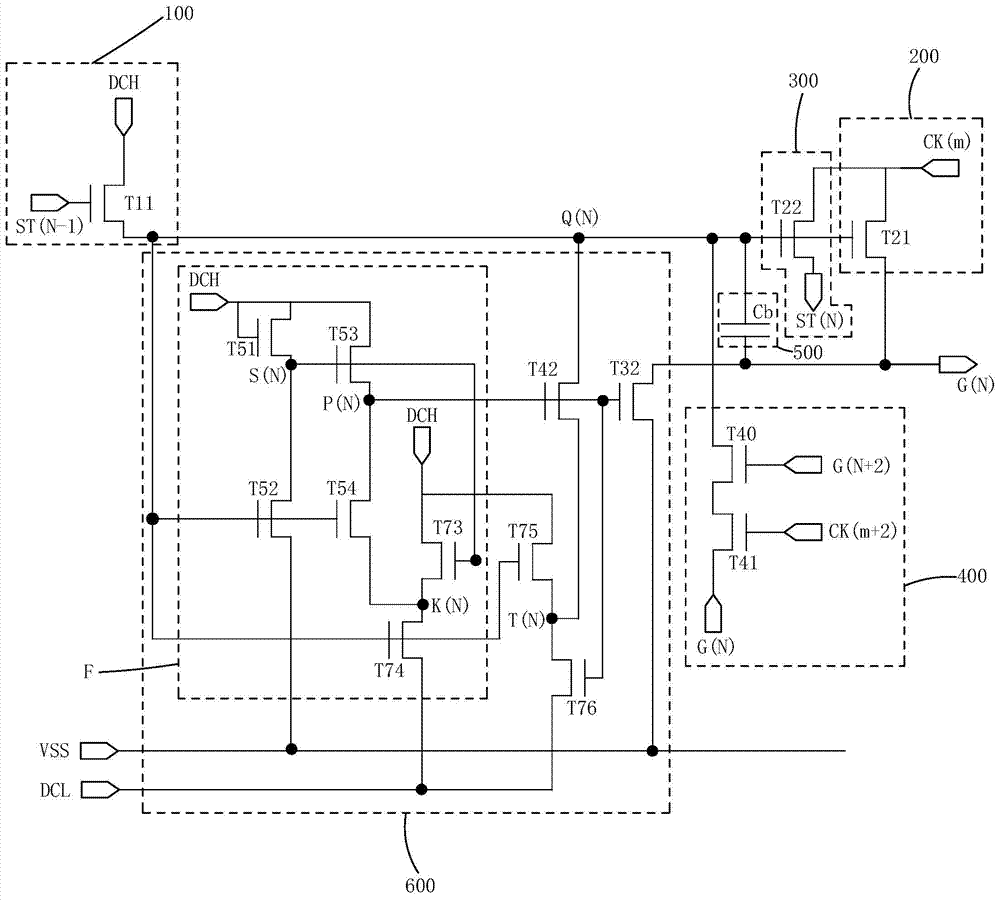
[0044] The invention provides a GOA circuit based on an oxide semiconductor thin film transistor. see figure 2 , is the circuit diagram of the first embodiment of the GOA circuit based on oxide semiconductor thin film transistors in the present invention, including multiple GOA unit circuits cascaded, and each level of GOA unit circuits includes: a pull-up control module 100, a pull-up module 200 , the downlink module 300 , the first pull-down module 400 , the bootstrap capacitor module 500 , and the pull-down maintenance module 600 .

[0045] Let N be a positive integer, except for the first-level GOA unit circuit, in the N-level GOA unit circuit:

[0046] The pull-up control module 100 includes an eleventh thin film transistor T11, the ga...


PUM


Abstract

The invention provides a gate driver on array (GOA) circuit based on an oxide semiconductor thin-film transistor. The electricity leakage can be prevented and reliability of the GOA circuit can be improved. A gate and a source electrode of a fortieth thin-film transistor (T40) in a first pull-down module (400) are in short circuit, thereby avoiding crosstalk current occurrence caused by a GOA unit circuit during an inactive period; a gate and a drain electrode of a seventy-fifth thin-film transistor (T75) in a pull-down holding module (600) are electrically connected to a first node (Q(N)), thereby preventing the influence on pull-down holding of the first node (Q(N)) by a constant-voltage high level (DCH); and a clearing and resetting module (700) is arranged and is used for carrying out clearing and resetting on the first node (Q(N)) before generation of each frame of picture, thereby eliminating the interference on the GOA circuit by residual charges and guaranteeing the normal output and normal picture display of the GOA circuit.

Description

technical field [0001] The invention relates to the field of driving liquid crystal displays, in particular to a GOA circuit based on an oxide semiconductor thin film transistor. Background technique [0002] A Liquid Crystal Display (LCD) has many advantages such as a thin body, power saving, and no radiation, and has been widely used. Such as: LCD TV, mobile phone, personal digital assistant (PDA), digital camera, computer screen or notebook computer screen, etc., occupy a dominant position in the field of flat panel display. [0003] Most of the liquid crystal displays currently on the market are backlight liquid crystal displays, which include a liquid crystal display panel and a backlight module. The working principle of the liquid crystal display panel is to pour liquid crystal molecules between the thin film transistor array substrate (Thin Film Transistor Array Substrate, TFT Array Substrate) and the color filter substrate (Color Filter, CF), and apply driving force...

Claims


Application Information

Patent Timeline
IPC IPC(8): G09G3/36
CPCG09G3/3677G09G2230/00G09G2300/0408G09G2300/0417G09G2310/0286G11C19/287G09G3/3266G09G3/36G09G2320/0214G09G2310/061
Inventor 戴超
Owner SHENZHEN CHINA STAR OPTOELECTRONICS TECH CO LTD
Why Eureka
Try Eureka