Fingerprint identification chip packaging structure and packaging method

A technology of fingerprint recognition and packaging method, which is applied in character and pattern recognition, acquisition/organization of fingerprints/palmprints, instruments, etc. It can solve the problems of fingerprint recognition device manufacturing and application limitations, fingerprint recognition chip sensitivity requirements are high, etc., to achieve size Effects of downscaling, increased sensitivity, and reduced thickness

Inactive Publication Date: 2015-08-19
CHINA WAFER LEVEL CSP
View PDF6 Cites 22 Cited by
  • Summary
  • Abstract
  • Description
  • Claims
  • Application Information

AI Technical Summary

Problems solved by technology

[0005] However, in the existing fingerprint identification devices, the sensitivity of the fingerprint identificati

Method used


Image

  • Fingerprint identification chip packaging structure and packaging method
  • Fingerprint identification chip packaging structure and packaging method
  • Fingerprint identification chip packaging structure and packaging method

Examples


Embodiment Construction

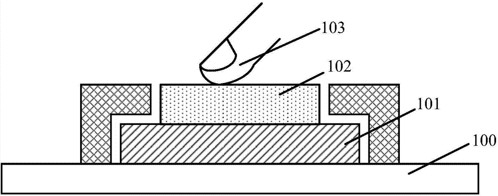
[0041] As mentioned in the background, the fingerprint identification chip needs to have higher sensitivity.

[0042] After research, please continue to refer to figure 1, the surface of the fingerprint identification chip 101 is covered with a glass substrate 102, the glass substrate 102 is used to protect the fingerprint identification chip 101, and the user's finger 103 is directly in contact with the glass substrate 102, therefore, in order to ensure that the glass substrate 102 has For sufficient protection capability, the thickness of the glass substrate 102 is relatively thick. However, since the glass substrate 102 is relatively thick, the fingerprint recognition chip 101 is required to have high sensitivity, so as to ensure that the user's fingerprint can be accurately extracted. However, it is difficult to manufacture a high-sensitivity fingerprint recognition chip, and the manufacturing cost is high, which in turn limits the application and promotion of the fingerp...


PUM


Abstract

The invention provides a fingerprint identification chip packaging structure and a packaging method. The packaging method comprises the steps that a substrate is provided; an induction chip is coupled at the surface of the substrate, the induction chip is provided with a first surface and a second surface which is opposite to the first surface, the second surface of the induction chip is arranged at the surface of the substrate, the first surface of the induction chip comprises induction areas and peripheral areas surrounding the induction areas, grooves are formed in the peripheral areas, the surfaces of the side walls and the bottom parts of the grooves and the surface of the peripheral areas are provided with re-wiring layers, and the side walls of the induction chip are exposed out of the grooves; and a plastic packaging layer is formed at the surface of the substrate, the plastic packaging layer surrounds the induction chip, the plastic packaging layer fills the grooves, and the plastic packaging layer is exposed out of the surface of the induction areas. Sensitivity of the induction chip in the packaging structure is enhanced, and the size of the packaging structure is reduced.

Description

technical field [0001] The invention relates to the technical field of semiconductor manufacturing, in particular to a packaging structure and packaging method of a fingerprint identification chip. Background technique [0002] With the progress of modern society, the importance of personal identification and personal information security has gradually attracted people's attention. Due to the uniqueness and invariance of human fingerprints, fingerprint identification technology has the characteristics of good security, high reliability, and simple and convenient use, making fingerprint identification technology widely used in various fields to protect personal information security. With the continuous development of science and technology, the information security of various electronic products has always been one of the key points of technological development. Especially for mobile terminals, such as mobile phones, notebook computers, tablet computers, digital cameras, etc...

Claims


Application Information

Patent Timeline
IPC IPC(8): H01L23/31H01L23/528H01L21/50H01L21/56G06K9/00
CPCH01L2924/181H01L24/05H01L2224/48091H01L2924/10157H01L2224/02371H01L2924/10156H01L2224/05569H01L2224/04042H01L2224/32225H01L2224/45124H01L2224/45139H01L2224/45147H01L2224/45184H01L2224/48227H01L2224/73265H01L2224/92247H01L2224/94H01L23/3185H01L2224/45144H01L24/45G06V40/1329H01L2924/00012H01L2924/00014H01L2224/03H01L2924/00G06V40/12H01L23/31
Inventor 王之奇杨莹喻琼王蔚
Owner CHINA WAFER LEVEL CSP
Why Eureka
Try Eureka