A kind of manufacturing method of large size precision circuit board

A production method and circuit board technology, which is applied in the manufacture of multilayer circuits, etc., can solve the problems of insufficient line width and open circuits in densely populated areas, and achieve the effects of avoiding poor exposure, accurate alignment, and avoiding misalignment

Active Publication Date: 2018-02-02
JIANGMEN SUNTAK CIRCUIT TECH
View PDF3 Cites 0 Cited by
  • Summary
  • Abstract
  • Description
  • Claims
  • Application Information

AI Technical Summary

Problems solved by technology

[0003] The present invention aims at the problems of insufficient line width and open circuits in the densely populated areas of the prior art in the production of large-scale precision circuit boards, and provides a method for producing circuit boards with a line spacing of less than 0.1 mm and a board length greater than 914 mm

Method used


Image

  • A kind of manufacturing method of large size precision circuit board
  • A kind of manufacturing method of large size precision circuit board
  • A kind of manufacturing method of large size precision circuit board

Examples


Embodiment

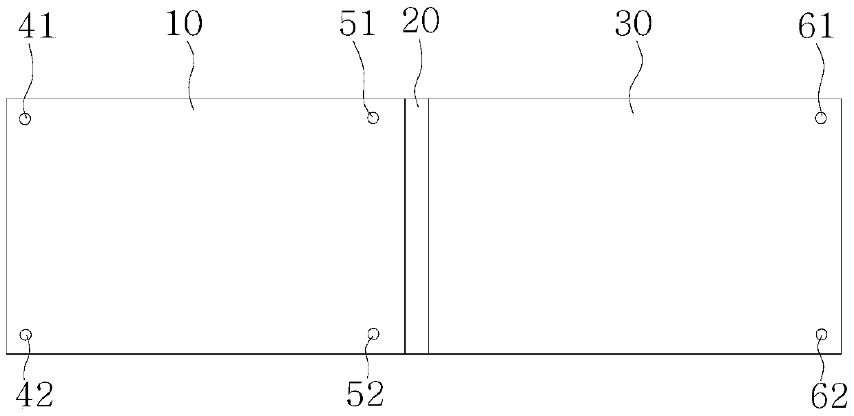
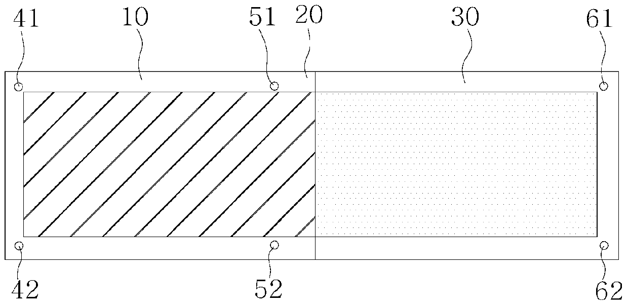
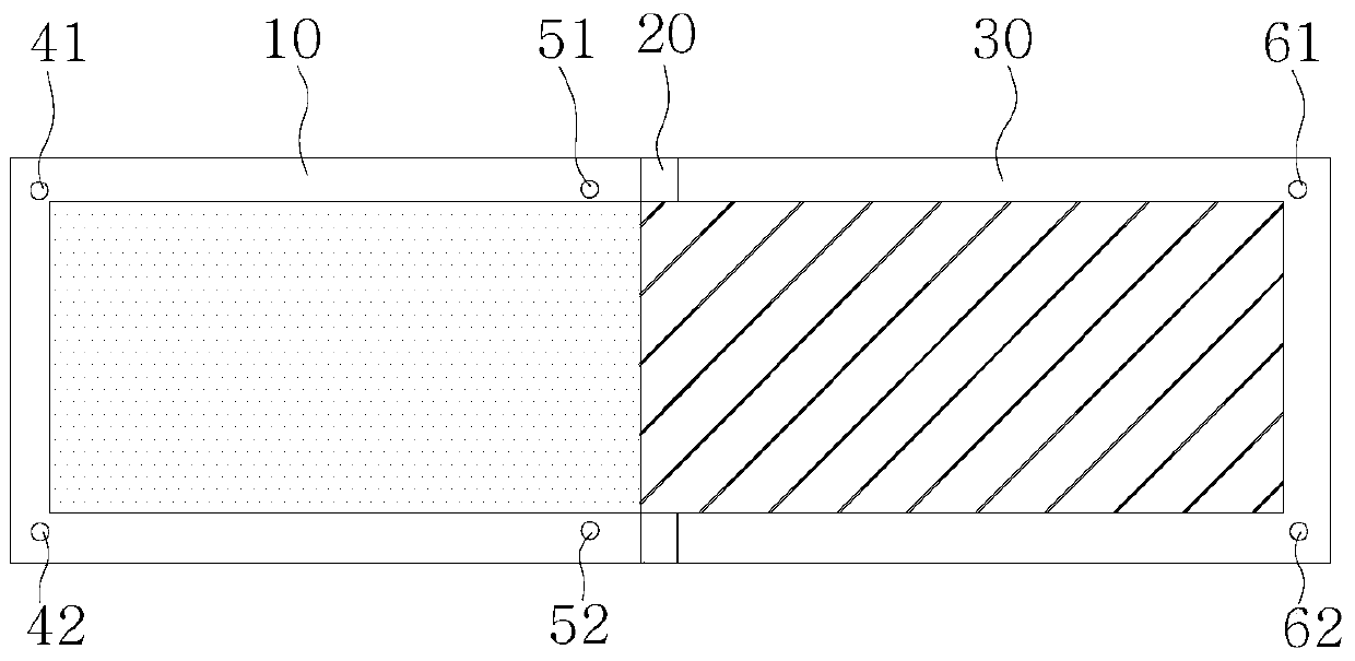
[0021] Reference Figure 1-3 This embodiment provides a method for manufacturing a large-size precision circuit board. The length of the circuit board manufactured in this embodiment is 1000 mm, and the minimum wire pitch is 0.1 mm.

[0022] The specific production steps are as follows:

[0023] (1) According to the circuit board production process of the prior art, the base material is opened to obtain the substrate for preparing each inner layer board. After the conventional pre-treatment of the substrate, the steps of applying wet film on the substrate, exposing, developing, etching, and removing the film (negative film process) are carried out in sequence to produce the inner layer circuit pattern on the substrate, thereby making each inner layer board.

[0024] Check and evaluate the quality of each inner layer board through inner AOI.

[0025] (2) The inner layer board is browned by the existing inner layer board browning process before pressing, so that a layer of brown oxide ...


PUM


Abstract

The invention relates to the technical field of circuit board production, in particular to a production method of a large-scale precision circuit board. The present invention avoids the problem that the line width of the formed circuit pattern is reduced due to the height difference at the splicing overlap when two sheets of film are directly spliced ​​together so that they are not tightly bonded to the board by adopting the method of two exposures. Set the width of the overlapping area to 0.2mm, and pre-enlarge the line pattern on the second line film corresponding to the overlapping area by 0.05mm, which can ensure the alignment of the line pattern formed in the overlapping area by the first exposure and the second exposure Accurate, avoiding the problems of poor exposure and misalignment of the line pattern in the overlapping area. Through the method of the invention, not only the precision circuit board with the line distance less than 0.1 mm can be manufactured, but also the circuit board with the board length longer than 914 mm can be manufactured.

Description

Technical field [0001] The invention relates to the technical field of circuit board manufacturing, in particular to a method for manufacturing a large-size precision circuit board. Background technique [0002] Circuit board, also known as circuit board or printed circuit board, referred to as PCB (Printed Circuit Board), is one of the important parts of the electronics industry. It is the support of electronic components and the carrier of electrical connections. With the continuous update of electronic product application technology and the improvement of functions, the design of circuit boards is becoming more and more precise, dense, high-performance and diversified, and the length of the circuit board is no longer limited to 813mm. However, in the existing circuit board production, the maximum length of the film is 813mm. If a circuit board with a length greater than 813mm is produced, two films need to be spliced ​​together, and then directly exposed again to make a circui...

Claims


Application Information

Patent Timeline
Patent Type & Authority Patents(China)
IPC IPC(8): H05K3/46
CPCH05K3/46
Inventor 胡志勇白会斌汪广明罗家伟
Owner JIANGMEN SUNTAK CIRCUIT TECH
Why Eureka
Try Eureka