
Chip image recognition device and method

An image recognition device and image recognition technology, applied in the directions of transportation and packaging, conveyor objects, electrical components, etc., can solve the problems of affecting the speed of the whole machine, damage to the chip, and the time spent on chip recognition alone, and achieve product quality improvement. The effect of average running speed

Inactive Publication Date: 2015-09-09
FOSHAN BLUE ROCKET ELECTRONICS
View PDF11 Cites 4 Cited by
  • Summary
  • Abstract
  • Description
  • Claims
  • Application Information

AI Technical Summary

Problems solved by technology

[0004] This method of chip identification is simple and practical, but the disadvantage is that the chip identification alone takes time, which affects the speed of the whole machine; Still stays on the high temperature furnace, so if heated for a long time, it may damage the chip

Method used


Image

  • Chip image recognition device and method
  • Chip image recognition device and method
  • Chip image recognition device and method

Examples


Embodiment Construction

[0045] The present invention will be further described below in conjunction with the accompanying drawings and embodiments.

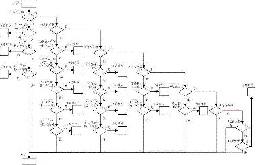
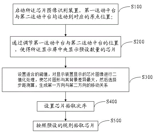
[0046] The present invention aims at the problem that chip recognition in the traditional technology takes time alone, affects the speed of the whole machine, and unqualified chips affect the chip pick-up speed, and provides a chip image recognition device and method, by quickly identifying and moving the chip to The center of the display device can identify the quality of multiple chips at the same time, and after picking up a qualified chip, quickly move the next qualified chip to the center of the display device in a certain order, so it hardly takes up the running time of the whole machine to identify whether the chip is good or bad , so the average running speed of the automatic chip bonder is improved, which is conducive to the improvement of product quality.

[0047] In order to have a clearer understanding of the technical features, purposes and...


PUM


Abstract

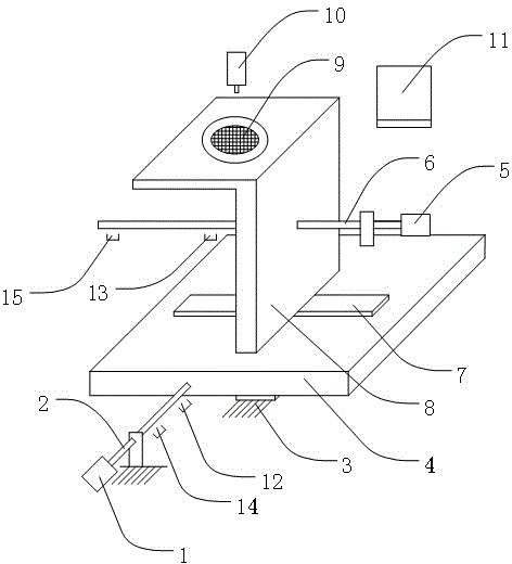
The invention provides a chip image recognition device and method. The chip image recognition device comprises a first driving mechanism, a first conducting mechanism, a first guide rail, a first movement platform, a second driving mechanism, a second conducting mechanism, a second guide rail, a second movement platform, wafers, an image photographing device and a display device. The first driving mechanism drives the first movement platform to move on the first guide rail along a first direction via the first conducting mechanism. The second driving mechanism drives the second movement platform to move on the second guide rail along a second direction via the second conducting mechanism. The first movementdirection is perpendicular to the second movement direction. The wafers are fixed on the chip image recognition device and move in the first direction and the second direction along with the first movement platform and the second movement platform. The image photographing device is arranged above the wafers and used for photographing images of multiple chips in real time simultaneously. The display device is connected with the image photographing device and used for displaying the images photographed by the image photographing device.

Description

technical field [0001] The invention relates to the field of semiconductor packaging equipment, and more specifically, to a chip image recognition device and method. Background technique [0002] In semiconductor device packaging, the automatic chip bonder first identifies whether the chip is good or bad, and then moves the qualified chip to the middle of the screen, and then the welding head picks up the chip and bonds the chip to the frame. Therefore, the time for the host to recognize the chip and move the qualified chip to the center of the screen determines the operating speed of the automatic die bonder. [0003] Generally, after the automatic die bonder picks up a chip, it moves the next chip to the center of the screen in the horizontal direction (or vertical direction) in turn, and then performs chip recognition. If it is qualified, the welding head will pick up the chip and stick it to the frame; if it is unqualified, move the next chip to the center of the screen...

Claims


Application Information

Patent Timeline
Patent Type & Authority Applications(China)
IPC IPC(8): H01L21/66H01L21/68H01L21/677H01L21/67H01L21/687
CPCH01L21/67259H01L21/67703H01L21/68H01L21/687H01L22/26
Inventor 姚剑锋张顺曾威徐周肖峰周名旷
Owner FOSHAN BLUE ROCKET ELECTRONICS
Learn More