A kind of growth method of light-emitting diode epitaxial wafer and epitaxial wafer

A technology for light emitting diodes and a growth method, which is applied to the growth method of light emitting diode epitaxial wafers and the field of epitaxial wafers, can solve the problems of limited luminous efficiency of LEDs, etc., and achieve the effects of rapid and sufficient reaction, high mobility and high luminous intensity

Active Publication Date: 2018-01-09
HC SEMITEK SUZHOU
View PDF3 Cites 0 Cited by
  • Summary
  • Abstract
  • Description
  • Claims
  • Application Information

AI Technical Summary

Problems solved by technology

[0006] In order to solve the problem of limited luminous efficiency of LEDs in the prior art, an embodiment of the present invention provides a method for growing an epitaxial wafer of a light emitting diode and an epitaxial wafer

Method used


Image

  • A kind of growth method of light-emitting diode epitaxial wafer and epitaxial wafer
  • A kind of growth method of light-emitting diode epitaxial wafer and epitaxial wafer

Examples


Embodiment 1

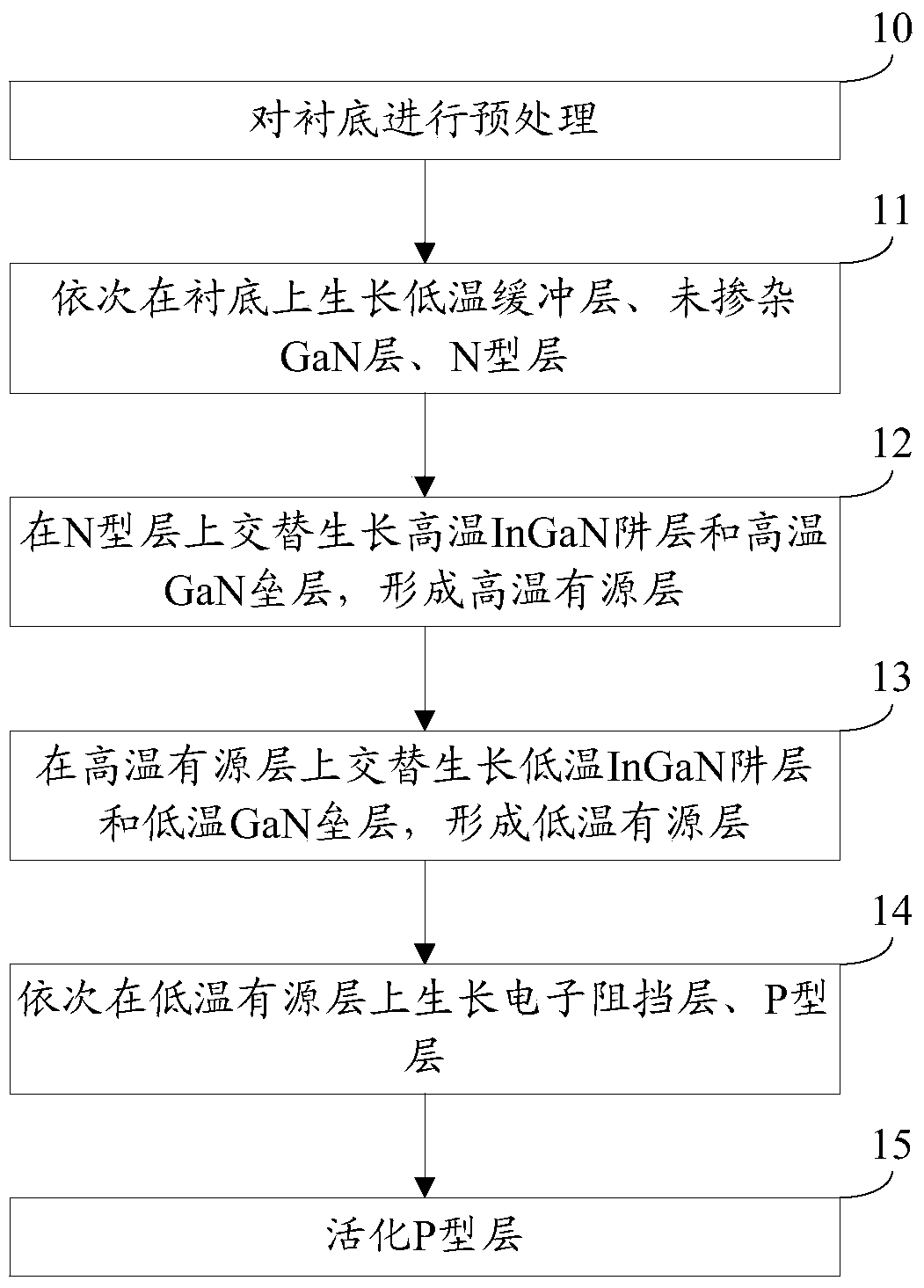
[0036] The embodiment of the present invention provides a growth method of a light emitting diode epitaxial wafer, see figure 1 , The growth method includes:

[0037] Step 10: Pre-treat the substrate.

[0038] Optionally, the substrate is sapphire.

[0039] Specifically, this step 10 may include:

[0040] Under a hydrogen atmosphere, process the substrate at a high temperature for 5-8 minutes. Among them, the temperature of the reaction chamber is 1000-1050°C, and the pressure of the reaction chamber is controlled at 200-300torr.

[0041] Step 11: Growing a low-temperature buffer layer, an undoped GaN layer, and an N-type layer on the substrate in sequence.

[0042] In this embodiment, a Veeco K465i / C4 MOCVD (Metal Organic Chemical Vapor Deposition, metal organic chemical vapor deposition) equipment is used to implement the LED epitaxial wafer growth method. Using high purity H 2 (Hydrogen) or high purity N 2 (Nitrogen) or high purity H 2 And high purity N 2 Mixed gas as carrier gas, h...

Embodiment 2

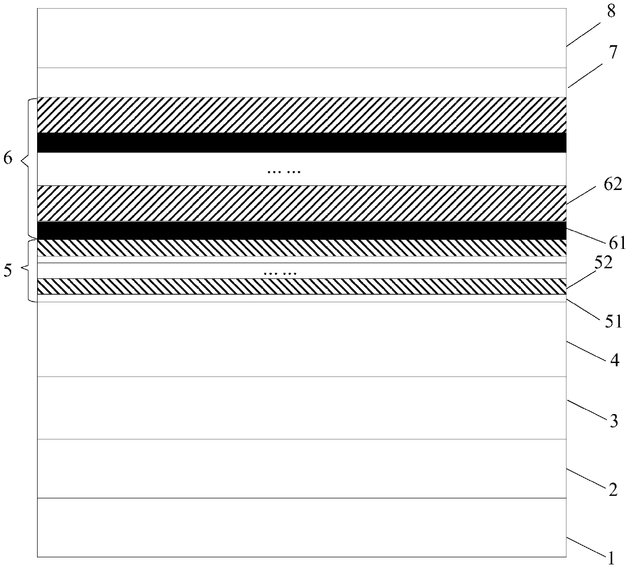
[0083] The embodiment of the present invention provides a light-emitting diode epitaxial wafer, which is obtained by using the light-emitting diode epitaxial wafer growth method provided in the first embodiment, see figure 2 The light-emitting diode epitaxial wafer includes a substrate 1, and a low-temperature buffer layer 2, an undoped GaN layer 3, an N-type layer 4, a high-temperature active layer 5, a low-temperature active layer 6, and electronic components sequentially stacked on the substrate 1. Barrier layer 7, P-type layer 8.

[0084] In this embodiment, the high-temperature active layer 5 is formed of a high-temperature InGaN well layer 51 and a high-temperature GaN barrier layer 52 that are grown alternately. The low-temperature active layer 6 is formed of a low-temperature InGaN well layer 61 and a low-temperature GaN barrier layer 62 that are alternately grown.

[0085] Among them, the growth temperature of the low temperature InGaN well layer 61 is lower than the gro...


PUM


Abstract

The invention discloses a growing method of an epitaxial wafer of a light emitting diode and the epitaxial wafer, and belongs to the field of semiconductor technology. The growing method comprises steps of growing a low-temperature buffering layer, a non-doping GaN layer, an N type layer, a high-temperature active layer, a low-temperature active layer, an electronic blocking layer and a P type layer on a substrate, wherein growing temperature and growing speed of a low-temperature InGaN trap layer are lower than those of a high-temperature InGaN trap layer; growing temperature and growing speed of a low-temperature GaN barrier layer are lower than those of a high-temperature GaN barrier layer; the thickness of the low-temperature InGaN trap layer is larger than that of the high-temperature InGaN trap layer; the thickness of the low-temperature GaN barrier layer is higher than that of the high-temperature GaN barrier layer; the V / III ratio of the low-temperature InGaN trap layer is different from that of the low-temperature GaN barrier layer; and the V / III ratio of the high-temperature InGaN trap layer is the same as that of the high-temperature GaN barrier layer. According to the invention, light emitting efficiency is high.

Description

Technical field [0001] The present invention relates to the field of semiconductor technology, in particular to a growth method of a light emitting diode epitaxial wafer and an epitaxial wafer. Background technique [0002] LED (Light Emitting Diode, light-emitting diode) is a semiconductor electronic component that can emit light. As a new type of high-efficiency, environmentally friendly, green solid-state lighting source, LED has the advantages of low voltage, low power consumption, small size, light weight, long life, high reliability, etc., and is being rapidly and widely used, such as traffic lights, automobiles Interior and exterior lights, urban landscape lighting, mobile phone backlights, outdoor full-color displays, etc. [0003] The epitaxial wafer is an important part of manufacturing LED. The existing epitaxial wafer growth method includes: sequentially growing a low-temperature buffer layer, an undoped GaN layer, an N-type layer, an active layer, and a P-type layer ...

Claims


Application Information

Patent Timeline
Patent Type & Authority Patents(China)
IPC IPC(8): H01L33/32H01L33/02
CPCH01L33/0075H01L33/02H01L33/32
Inventor 从颖姚振韩杰陈柏松胡加辉魏世祯
Owner HC SEMITEK SUZHOU
Why Eureka
Try Eureka