P-type nitride epitaxial structure, preparation method and semiconductor device

An epitaxial structure, nitride technology, applied in semiconductor/solid-state device manufacturing, electrical components, final product manufacturing, etc., can solve the problem that the self-compensation effect of doping elements cannot be suppressed, the carrier concentration decreases, and the activation rate of doping elements is low. and other problems, to achieve the effect of promoting good surface morphology, inhibiting self-compensation effect, and increasing solubility

Active Publication Date: 2022-05-17
JIANGSU INST OF ADVANCED SEMICON CO LTD
View PDF7 Cites 0 Cited by
  • Summary
  • Abstract
  • Description
  • Claims
  • Application Information

AI Technical Summary

Problems solved by technology

There are two main reasons for the low carrier concentration of P-type GaN materials. On the one hand, the activation rate of doping elements is low; on the other hand, traditional doping methods cannot suppress the self-compensation of doping elements. The concentration of heteroelements often causes the carrier concentration of P-type GaN materials to decrease instead.

Method used


Image

  • P-type nitride epitaxial structure, preparation method and semiconductor device
  • P-type nitride epitaxial structure, preparation method and semiconductor device
  • P-type nitride epitaxial structure, preparation method and semiconductor device

Examples


preparation example Construction

[0052] The above P-type nitride epitaxial structure can be prepared by the following preparation method, including the following steps:

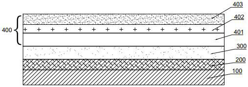
[0053] S1. Growing a U-shaped nitride layer 200 on the substrate 100;

[0054] Specifically, a U-shaped nitride layer 200 of 1 μm-3 μm is grown on the substrate; the U-shaped nitride layer 200 makes the heterogeneous substrate transition to a flat GaN material layer;

[0055] S2. Growing a P-type nitride prelayer 300 on the U-type nitride layer 200, wherein the P-type nitride prelayer 300 is lightly doped with Mg;

[0056] Specifically, a P-type nitride prelayer 300 of 0.5um-1.5μm is grown on the U-type nitride layer 200; wherein, the doping concentration of the Mg element in the P-type nitride prelayer 300 is 1E18cm -3 -1E19cm -3 ;

[0057] The lightly doped P-type nitride pre-layer 300 avoids the weak N-type influence of the U-type nitride layer on the subsequent P-type layer, and eliminates the influence of the depletion layer; and the...

Embodiment 1

[0070] This embodiment prepares and tests the P-type GaN epitaxial structure, specifically including the following steps:

[0071] 1) Grow a 2um U-shaped GaN layer on a sapphire substrate;

[0072] 2) Grow a 1um P-type GaN front layer on the U-type GaN layer, in which the doping concentration of Mg is about 1E19cm -3 ;

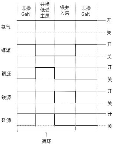
[0073] 3) Set the growth temperature to 1050°C, feed the gallium source, and grow the non-doped GaN layer for 15s;

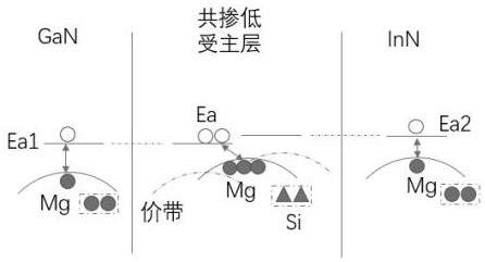
[0074] 4) Turn off the gallium source, pass in the indium source and the silicon source, cool down to 950°C to grow the co-doped low acceptor layer, and the growth time is 5s, where In / Ga (molar ratio) = 2, and the doping concentration of Si is 5E17cm -3 ;

[0075] 5) Turn off the indium source and the silicon source, and only pass in the magnesium source, grow the Mg-doped incorporation layer, and the growth time is 5s, in which the doping concentration of Mg is 5E20cm -3 ;

[0076] 6) According to steps 3), 4), and 5), grow 200 cycles to ...

Embodiment 2

[0094] In order to further illustrate the role of the P-type GaN pre-layer in the present invention, the thickness of the P-type GaN pre-layer is changed in this embodiment compared with Embodiment 1, and the rest is the same as that of Embodiment 1;

[0095] Result: Under the test condition of the Hall current of 1uA, the Hall effect test is carried out:

[0096] 1) When the thickness of the P-type GaN front layer is 0.5um, the doping concentration of Mg is about 1E18cm -3 , the carrier concentration of the prepared P-type GaN layer is 5.4E18cm -3 ;

[0097] 2) When the thickness of the P-type GaN front layer is 1.5um, the doping concentration of Mg is about 1E19cm -3 , the carrier concentration of the prepared P-type GaN layer is 6.2E18cm -3 ;

[0098] The results show that: compared with the non-P-type GaN pre-layer of Comparative Example 1, the carrier concentration of the two kinds of thickness pre-layers in Example 2 is improved, which further proves that the P-type ...


PUM

PropertyMeasurementUnit
thicknessaaaaaaaaaa
thicknessaaaaaaaaaa
thicknessaaaaaaaaaa

Abstract

The invention discloses a P-type nitride epitaxial structure, a preparation method and a semiconductor device. The P-type nitride epitaxial structure comprises a substrate; the U-type nitride layer, the P-type nitride preposed layer and the P-type nitride composite layer are sequentially grown on the substrate; wherein the P-type nitride front layer is a nitride layer lightly doped with Mg; the P-type nitride composite layer comprises a non-doped nitride layer, a co-doped low acceptor layer and a magnesium-doped incorporated layer which are of a periodic structure, and the non-doped nitride layer, the co-doped low acceptor layer and the magnesium-doped incorporated layer grow in sequence in a single period; the magnesium-doped incorporated layer is a nitride layer heavily doped with Mg; and the co-doped low acceptor layer is a Si-doped indium nitride layer. According to the invention, the self-compensation effect of the dopant can be inhibited and the activation rate of the dopant can be improved, so that the carrier concentration of the P-type nitride material is improved.

Description

technical field [0001] The invention relates to the technical field of semiconductors, in particular to a P-type nitride epitaxial structure, a preparation method and a semiconductor device. Background technique [0002] Due to its excellent characteristics, GaN material has become an important material for manufacturing light-emitting devices, high-temperature and high-power devices and ultraviolet detectors. P-type doping is an essential part of manufacturing GaN devices, so it has attracted the attention of many research groups. [0003] Although the technology has been continuously developed in recent years, the current carrier concentration of P-type GaN materials in the industry is still much lower than that of N-type GaN. With the development of high-performance GaN devices, the limitation has become more and more serious. There are two main reasons for the low carrier concentration of P-type GaN materials. On the one hand, the activation rate of doping elements is l...

Claims


Application Information

Patent Timeline
Patent Type & Authority Applications(China)
IPC IPC(8): H01L21/02
CPCH01L21/0254H01L21/0257H01L21/02458H01L21/0262Y02P70/50
Inventor 王国斌周溯沅
Owner JIANGSU INST OF ADVANCED SEMICON CO LTD
Why Eureka
Try Eureka