

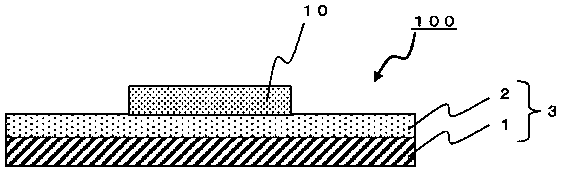
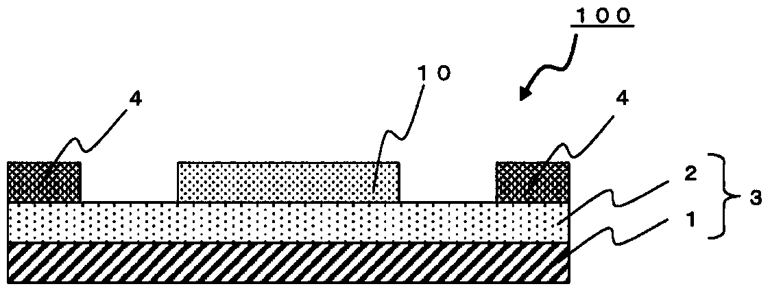
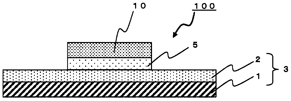
Film for forming protective film and composite sheet for forming protective film
A protective film, polymer technology, applied in applications, home appliances, other home appliances, etc., can solve problems such as poor transportation, wafer bending, poor shrinkage, etc., to achieve high reliability and correct the effect of bending
- Summary
- Abstract
- Description
- Claims
- Application Information
AI Technical Summary
Problems solved by technology
Method used
Image

Examples
Embodiment
[0179] Hereinafter, although an Example demonstrates this invention, this invention is not limited to these Examples. In addition, in the following examples or comparative examples, , , , and .
[0180]
[0181] Laminate 4 films for forming a protective film with a thickness of 45 μm, heat-cure in an oven in an air atmosphere (130°C for 2 hours), and produce a test strip cut into a strip with a width of 4.5 mm, a length of 20.0 mm, and a thickness of 0.18 mm piece.
[0182]Using a viscoelasticity measuring device (DMA Q800 from TA instruments company), in tensile mode, with a frequency of 11 Hz and a heating rate of 3 °C / min, the tan δ (loss elastic modulus and storage modulus of elasticity). In this temperature range, the temperature at which tan δ showed the maximum value was read, and this was made the glass transition temperature (Tg) after thermal curing of the film for protective film formation.
[0183]
[0184] The storage elastic modulus at 23°C of the measure...
PUM
| Property | Measurement | Unit |
|---|---|---|
| glass transition temperature | aaaaa | aaaaa |
| particle size | aaaaa | aaaaa |
| glass transition temperature | aaaaa | aaaaa |
Abstract
Description
Claims
Application Information