Fingerprint recognition device and electronic equipment comprising fingerprint recognition device

A fingerprint recognition and fingerprint recognition module technology, which is applied in character and pattern recognition, instruments, computer parts, etc., can solve the problems of unsuitable thin and light applications, large amount of conductive materials used, complex spatial structure, etc., and improve the accuracy , cheap price, effect of reducing thickness

Inactive Publication Date: 2015-10-14
NANCHANG OUFEI BIOLOGICAL IDENTIFICATION TECH +3
View PDF5 Cites 3 Cited by
  • Summary
  • Abstract
  • Description
  • Claims
  • Application Information

AI Technical Summary

Problems solved by technology

Image feature recognition and laser feature recognition use visible light and laser to extract fingerprint ridge line information respectively, and use algorithms for feature analysis to identify different individuals; both methods require more complex spatial structures such as CCD probes and laser generators. Not suitable for thin and light applications
[0005] However, the structure of the capacitive fingerprint sensor in the prior art is a silicon substrate structure, and its driving electrodes and sensing electrodes are ITO structures, that is, conductive materials are directly coated on the substrate to form conductive patterns, so that the amount of conductive materials used is large. , and easy to wear; in addition, the conductive material used in the prior art is indium tin oxide, and indium in indium tin oxide is a rare metal and expensive

Method used


Image

  • Fingerprint recognition device and electronic equipment comprising fingerprint recognition device
  • Fingerprint recognition device and electronic equipment comprising fingerprint recognition device
  • Fingerprint recognition device and electronic equipment comprising fingerprint recognition device

Examples


Embodiment Construction

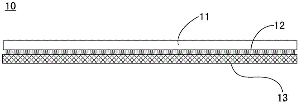
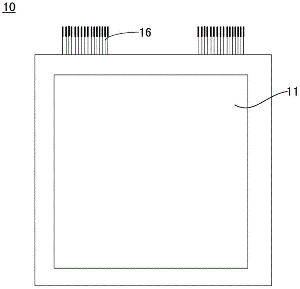
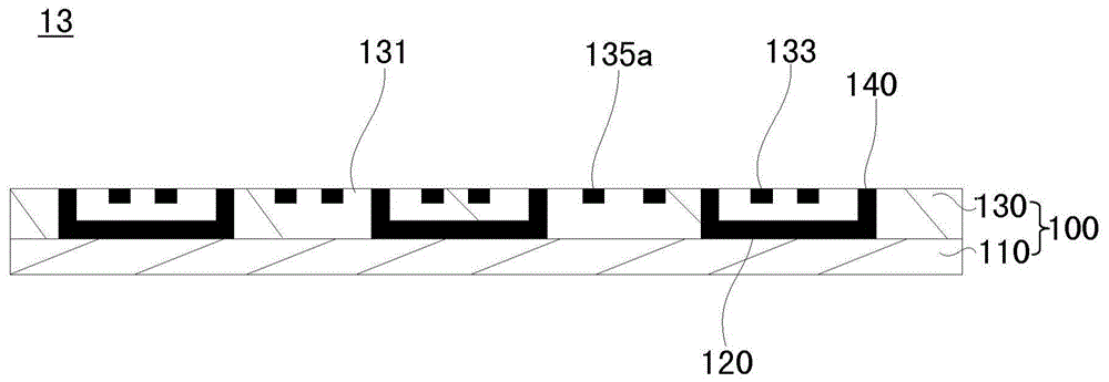
[0036] Example embodiments will now be described more fully with reference to the accompanying drawings. However, the example embodiments can be implemented in various forms, and should not be construed as being limited to the embodiments set forth herein; on the contrary, these embodiments are provided so that the present invention will be comprehensive and complete, and fully convey the concept of the example embodiments To those skilled in the art. In the figure, the thickness of regions and layers are exaggerated for clarity. The same reference numerals in the figures indicate the same or similar structures, and thus their repeated description will be omitted.

[0037] The described features, structures or characteristics can be combined in one or more embodiments in any suitable way. In the following description, many specific details are provided to give a full understanding of the embodiments of the present invention. However, those skilled in the art should realize tha...


PUM


Abstract

The invention provides a fingerprint recognition device and electronic equipment comprising the fingerprint recognition device. The fingerprint recognition device comprises a fingerprint input module and a fingerprint recognition module, wherein the fingerprint recognition module comprises a dielectric layer, a plurality of driving channels, a plurality of sensing channels, a bypass module and a conducting module; the dielectric layer comprises reticular grooves; the reticular grooves are filled with conducting materials; the driving channels and the sensing channels are accommodated in the reticular grooves and are positioned on the same surface of the dielectric layer; the driving channels are in continuous arrangement in the first dimension direction; the sensing channels comprise a plurality of sensing units; the sensing units are in segmented arrangement in a second dimension direction intersected with the first dimension direction; the driving channels and the sensing channels are matched for forming a plurality of recognition units; the bypass module and the reticular grooves are not positioned on the same plane; and the conducting module is arranged between the reticular grooves and the bypass module and is used for electrically connecting the sensing units and the bypass module to form the continuous sensing channels.

Description

Technical field [0001] The present invention relates to fingerprint identification technology, in particular to a fingerprint identification device and electronic equipment containing the same. Background technique [0002] In recent years, with the development of storage technology, electronic devices such as mobile phones and computers store a large amount of personal information and other important data, and their security has become more important. At present, passwords, graphics, and other forms are often used to achieve password protection for their electronic devices, that is, users can set personal password protection by inputting numbers, letters and combinations of passwords in advance, or inputting specific graphics to electronic devices; When using an electronic device, enter these passwords or graphics again, and the electronic device authenticates the legitimacy of the user's identity by comparing with the preset password or graphics, thereby protecting the user's p...

Claims


Application Information

Patent Timeline
Patent Type & Authority Applications(China)
IPC IPC(8): G06K9/00
Inventor 张晟
Owner NANCHANG OUFEI BIOLOGICAL IDENTIFICATION TECH
Why Eureka
Try Eureka