OLED (Organic Light Emitting Diode) panel display defect restoration method

A defect repair and panel display technology, applied in the field of OLED display, can solve the problems of high operator requirements, accuracy rate dependent on artificial factors, and affecting the efficiency of OLED panel display defect inspection and repair, so as to improve accuracy rate, improve repair efficiency, and avoid The effect of repeated positioning

Inactive Publication Date: 2015-10-14
SICHUAN CCO DISPLAY TECH
View PDF6 Cites 16 Cited by
  • Summary
  • Abstract
  • Description
  • Claims
  • Application Information

AI Technical Summary

Problems solved by technology

Although this inspection and repair method is simple to operate and widely used because it is easy to use, there are some obvious display defects at the s

Method used


Image

  • OLED (Organic Light Emitting Diode) panel display defect restoration method

Examples


Embodiment Construction

[0008] In order to make the objectives, technical solutions and advantages of the present invention clearer, the present invention will be further described in detail below with reference to the accompanying drawings and embodiments. It should be understood that the specific embodiments described herein are only used to explain the present invention, but not to limit the present invention.

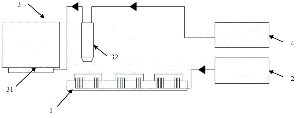
[0009] like figure 1 As shown, the OLED panel display defect repair method in this embodiment includes a vacuum adsorption platform 1, a lighting system 2, a display defect inspection device 3 and a laser generator 4, wherein the display defect inspection device 3 includes a display device 31, a microscope 32, CCD and adjustable platform, the microscope 32 is fixed on the adjustable platform and the image is displayed on the display device 31 through the CCD; the laser head of the laser generator 4 overlaps with the lens of the microscope 32 of the display defect inspection device 3, and t...


PUM


Abstract

The invention discloses an OLED (Organic Light Emitting Diode) panel display defect restoration method. The method comprises the following steps that when the OLED panel display defect restoration is required, firstly, an OLED panel is fixed on a vacuum absorption platform through vacuum; then, the OLED panel is lightened through a light-up system, at this moment, an approximate position of a repairable display defect can be determined by the lightened OLED panel, and the display defect is labeled; an adjustable platform of a display defect detection device is adjusted to move a microscope at a position above the display defect labeled in the previous step, the microscope is adjusted for accurately positioning the display defect, and image information of the display defect can be obtained through a display device; and a laser generator is opened, and under the real-time monitor and guidance of the display device, an emitted laser beam is utilized to display and accurately restore the defect.

Description

technical field [0001] The invention belongs to the technical field of OLED display, and particularly relates to a method for repairing display defects of an OLED panel. Background technique [0002] After the OLED panel completes the aging process, it is necessary to check and mark the display defects of the OLED panel, and repair the repairable display defects. At present, the commonly used inspection and repair methods are: first, manually hold the microscope to inspect the display defects; then, mark the display defects; third, transfer the marked substrate to the laser repair table to locate the display defects again; In four steps, laser repair is performed on the display defect part. Although this inspection and repair method is simple to operate and easy to use, it is widely used, but there are some obvious display defects at the same time. The accuracy of the OLED panel depends on artificial factors, which requires higher operators and artificially affects the pro...

Claims


Application Information

Patent Timeline
IPC IPC(8): G09G3/00
Inventor 朴章镐
Owner SICHUAN CCO DISPLAY TECH
Why Eureka
Try Eureka