Encapsulated thin film and manufacturing method therefor, light emitting apparatus, display panel and display device

一种封装薄膜、基板的技术,应用在电固体器件、半导体器件、有机半导体器件等方向,能够解决成本高、难应用曲面显示屏、封装玻璃难弯曲性等问题,达到良好兼容、好可弯曲性能的效果

Active Publication Date: 2015-10-14
BOE TECH GRP CO LTD
View PDF11 Cites 5 Cited by
  • Summary
  • Abstract
  • Description
  • Claims
  • Application Information

AI Technical Summary

Problems solved by technology

At present, the conventional encapsulation method of organic light-emitting devices is encapsulation by encapsulation glass, which can well serve the purpose of blocking water and oxygen, but the thickness of encapsulation glass is generally thick, and additional moisture-absorbing agents need to be attached, so that The thickness of the organic light-emitting device is increased, and due to the hardness and inflexibility of the packaging glass, it is difficult to apply this organic light-emitting device to the curved display screen, so the defects of the packaging method of the conventional organic light-emitting device are becoming more and more obvious
In the prior art, another alternative packaging method for organic light-emitting devices is the sequential deposition of organic and inorganic thin films. This method can achieve the purpose of flexibility and reduce the thickness of the device, but this method requires high vacuum conditions, step by step through expensive deposition equipment, generally at a higher cost

Method used


Image

  • Encapsulated thin film and manufacturing method therefor, light emitting apparatus, display panel and display device
  • Encapsulated thin film and manufacturing method therefor, light emitting apparatus, display panel and display device

Examples


Embodiment Construction

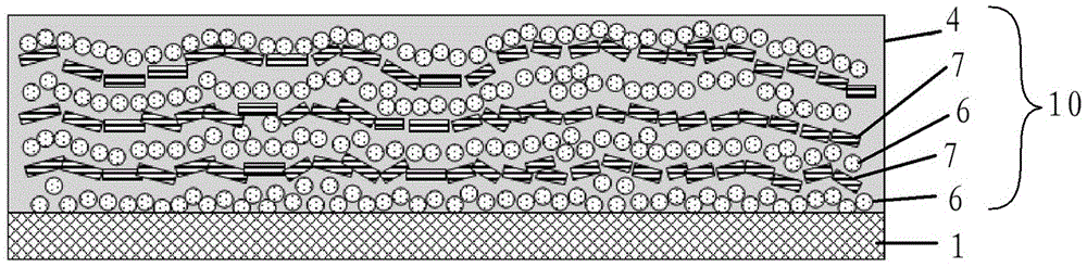
[0027] Below, reference will be made to the appended Figure 1-2 Various embodiments of the present invention are described in detail.

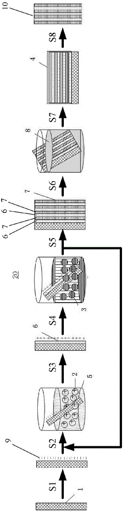
[0028] figure 2 is a flowchart 20 of making an encapsulation film according to one embodiment of the present invention. figure 2 The shown method of making the encapsulation film may comprise the following steps:

[0029] In step S1, the substrate 1 is pretreated so that its surface is positively charged or negatively charged. The substrate 1 is a conventional glass substrate or other deposition substrates. The pretreatment method used may be oxygen plasma treatment or other electrochemical treatment, the purpose of which is to make the surface of the substrate 1 be positively or negatively charged after the pretreatment. figure 2 As shown in step S1 of , the surface of the substrate 1 is negatively charged 9 after pretreatment. Alternatively, the surface of the substrate 1 may also be positively charged after pretreatment.

[0030] ...


PUM


Abstract

The invention relates to an encapsulated thin film and a manufacturing method therefor, a light emitting apparatus, a display panel and a display device. The encapsulated thin film comprises a nanometer material layer or a polycation organic material layer, a moisture absorption layer formed on the nanometer material layer or the polycation organic material layer and a sealing layer which is used for sealing the nanometer material layer or the polycation organic material layer and the moisture absorption layer. The encapsulated structure provided by the invention is formed by alternately assembling materials with different charges (the nanometer material layer or the polycation organic material layer and the moisture absorption layer). Compared to the vacuum coating method in the prior art, each layer of the encapsulated structure provided by the invention is soaked in a solution and is constructed by virtue of a self-assembling method without expensive vacuum equipment, so that the cost is obviously lowered, and the encapsulated structure is simple in preparation process and can be prepared in a large area.

Description

technical field [0001] The invention relates to a light-emitting device, in particular to an encapsulation film, a method for making the encapsulation film, a display panel and a display device. Background technique [0002] The encapsulation structure of the organic light emitting device is an important part of the organic light emitting device, because the encapsulation structure needs to block water and oxygen to protect the normal operation of the organic light emitting device. At present, the conventional encapsulation method of organic light-emitting devices is encapsulation by encapsulation glass, which can well serve the purpose of blocking water and oxygen, but the thickness of encapsulation glass is generally thick, and additional moisture-absorbing agents need to be attached, so that The thickness of the organic light emitting device is increased, and due to the hardness and inflexibility of the packaging glass, it is difficult to apply the organic light emitting ...

Claims


Application Information

Patent Timeline
Patent Type & Authority Applications(China)
IPC IPC(8): H01L51/52H01L51/56H01L27/32
CPCH10K59/00H10K50/844H10K71/00Y02E10/549Y02P70/50H10K50/846H10K50/8445H10K2102/331H10K77/10H10K50/8426
Inventor 石守磊洪晓雯
Owner BOE TECH GRP CO LTD
Why Eureka
Try Eureka