A kind of solid state disk and its read and write operation method

A technology for solid-state disk and read operation, which is applied in the direction of redundant code error detection, input/output to record carrier, generation of response error, etc. It can solve the problem of rising original bit error rate of solid-state disk, loss of oxide layer, short life, etc. problems, to achieve the effect of multi-level data redundancy, high original bit error rate, and improved service life

Active Publication Date: 2018-04-24
HUAZHONG UNIV OF SCI & TECH
View PDF6 Cites 0 Cited by
  • Summary
  • Abstract
  • Description
  • Claims
  • Application Information

AI Technical Summary

Problems solved by technology

The erasing and writing operation of the solid-state disk will wear out the oxide layer, causing electrons to escape from the oxide layer, resulting in an increase in the original bit error rate of the solid-state disk
When the raw bit error rate rises and the data reliability of the SSD cannot be guaranteed, the life of the SSD is exhausted
SSDs based on MLC flash memory chips have a higher raw bit error rate due to storing more bits of information in one memory cell, resulting in a shorter lifespan
At present, the industry improves the data reliability of solid-state disks by strengthening the in-page ECC verification capability, thereby prolonging the service life of solid-state disks, but at the same time it will increase the decoding delay of solid-state disks, and is limited by the number of bits in the spare area. length

Method used


Image

  • A kind of solid state disk and its read and write operation method
  • A kind of solid state disk and its read and write operation method
  • A kind of solid state disk and its read and write operation method

Examples


Embodiment Construction

[0033] In order to make the object, technical solution and advantages of the present invention clearer, the present invention will be further described in detail below in conjunction with the accompanying drawings and embodiments. It should be understood that the specific embodiments described here are only used to explain the present invention, not to limit the present invention. In addition, the technical features involved in the various embodiments of the present invention described below can be combined with each other as long as they do not constitute a conflict with each other.

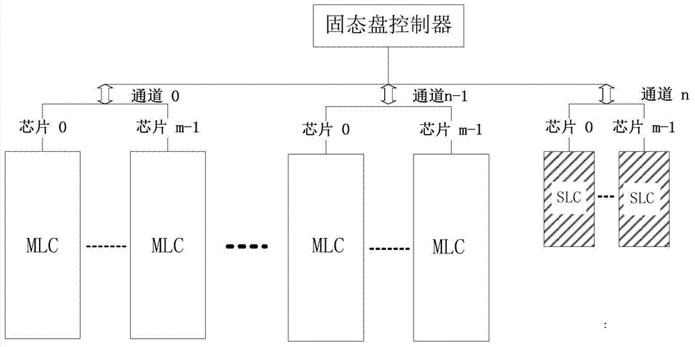
[0034] Such as figure 1 As shown, the solid state disk in the embodiment of the present invention includes a solid state disk controller, n+1 channels, m SLC flash memory chips and m×n MLC flash memory chips, and both m and n are positive integers. The solid-state disk controller is used to receive and process the read and write load requests of the upper layer, and send read and write requests...


PUM


Abstract

The invention discloses a solid-state disk and a reading and writing operation method thereof. The solid-state disk includes a solid-state disk controller, n+1 channels, m SLC flash memory chips and m×n MLC flash memory chips, where m and n are both positive integers; m SLC flash memory chips are set in n+1 channels On one of the channels, m×n MLC flash memory chips are set on the remaining n channels of the n+1 channels, and each of the remaining n channels has m MLC flash memory chips; SLC flash memory chips The storage capacity of the MLC flash memory chip is small for storing verification data, and the storage capacity of the MLC flash memory chip is large for storing user data. The SLC flash memory chip and the MLC flash memory chip perform data transmission through the channel where they are located. The invention can effectively improve the service life of the solid state disk and reduce the cost of the storage system.

Description

technical field [0001] The invention belongs to the technical field of computer storage, and more specifically relates to a solid-state disk and a read-write operation method thereof. Background technique [0002] Compared with traditional magnetic disks, solid-state disks based on flash memory chips have the advantages of high read and write speeds, low energy consumption, and shock resistance. In order to improve the capacity density of solid-state disks, multi-level cell (Multi-Level Cell, MLC) technology, that is, store two or more bits of information in one storage unit, is widely used in solid-state disks; at the same time, the process of solid-state disks Dimensions are continuing to shrink, which will lead to a decrease in the service life of SSDs. [0003] The lifespan of an SSD is primarily limited by its underlying structure. The memory cell of flash memory contains an oxide layer that can store electrons, showing different charge states according to the number ...

Claims


Application Information

Patent Timeline
Patent Type & Authority Patents(China)
IPC IPC(8): G06F3/06G06F11/10
Inventor 曹强万胜刚虞瑞荣谭诗诗
Owner HUAZHONG UNIV OF SCI & TECH
Why Eureka
Try Eureka