Light-emitting diode epitaxial wafer and manufacturing method thereof
A technology of light-emitting diodes and epitaxial wafers, applied in the direction of electrical components, circuits, semiconductor devices, etc., can solve problems such as insufficient current expansion of epitaxial wafers, and achieve the effects of avoiding lattice mismatch, reducing defects, and improving crystal quality
- Summary
- Abstract
- Description
- Claims
- Application Information
AI Technical Summary
Problems solved by technology
Method used
Image
Examples
Embodiment Construction
[0022] In order to make the object, technical solution and advantages of the present invention clearer, the implementation manner of the present invention will be further described in detail below in conjunction with the accompanying drawings.
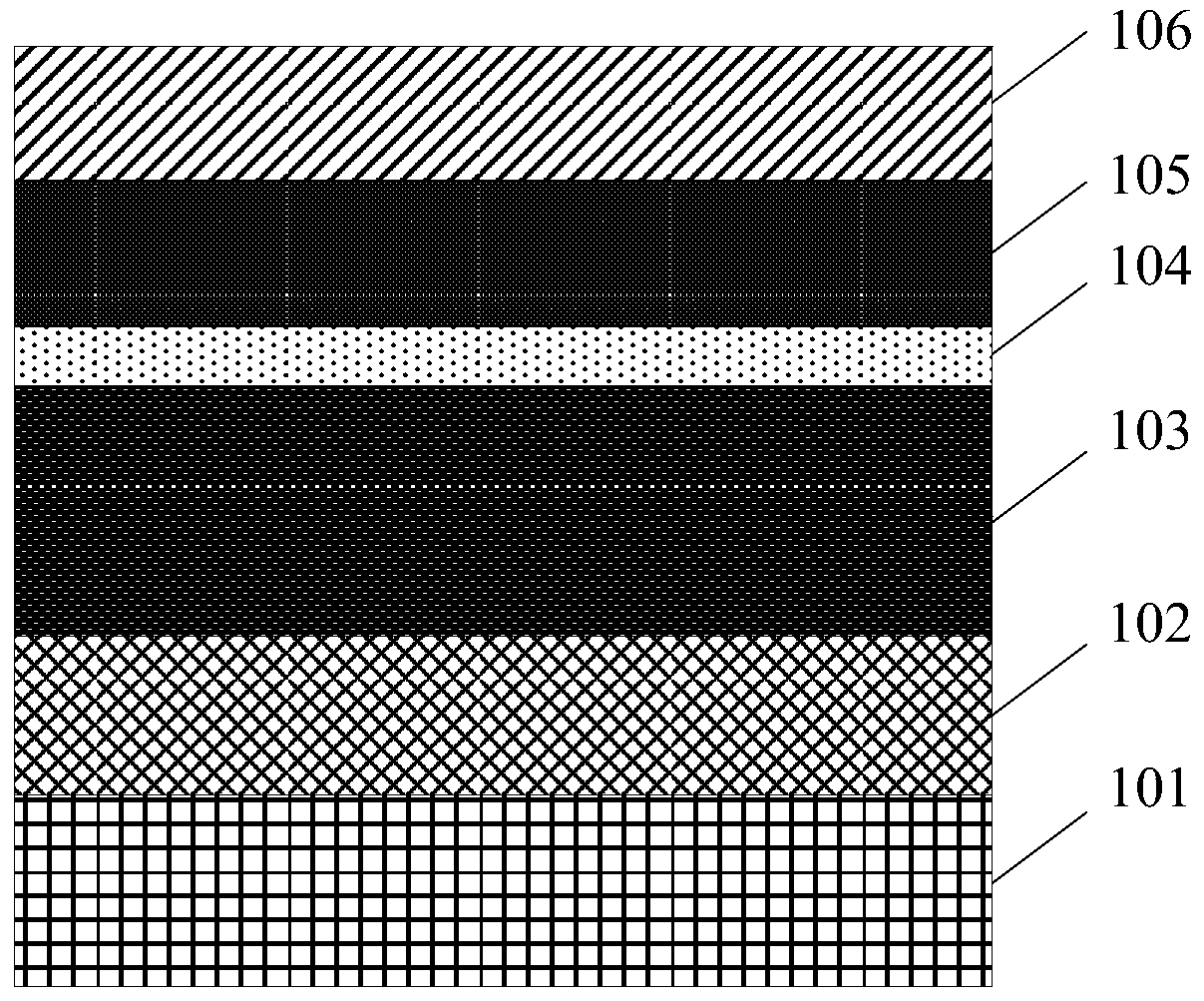
[0023] figure 1 is a schematic structural view of a light-emitting diode epitaxial wafer provided by an embodiment of the present invention, see figure 1 The light emitting diode epitaxial wafer includes a substrate 101 , an undoped layer 102 , an N-type layer 103 , an N-type current spreading layer 104 , a multi-quantum well layer 105 and a P-type layer 106 sequentially formed on the substrate 101 .
[0024] The N-type current spreading layer 104 includes an AlGaN / n-GaN superlattice structure, and the Al content of the AlGaN sublayer in the AlGaN / n-GaN superlattice structure increases layer by layer along the growth direction of the epitaxial wafer, The content of Al in the AlGaN sub-layer is 10%-80%.
[0025] Wherein, the AlGaN sub...
PUM
 Abstract
Description
Claims
Application Information

