A method for fabricating flexible nanocolumn arrays with high aspect ratio

A technology with high aspect ratio and manufacturing method, which is applied in the fields of nanotechnology, semiconductor/solid-state device manufacturing, photolithographic exposure device, etc.

Active Publication Date: 2017-12-12
NORTHWESTERN POLYTECHNICAL UNIV
View PDF2 Cites 0 Cited by
  • Summary
  • Abstract
  • Description
  • Claims
  • Application Information

AI Technical Summary

Problems solved by technology

However, the current research is not yet able to solve the problem of simple, efficient and high-precision flexible period production.

Method used


Image

  • A method for fabricating flexible nanocolumn arrays with high aspect ratio
  • A method for fabricating flexible nanocolumn arrays with high aspect ratio
  • A method for fabricating flexible nanocolumn arrays with high aspect ratio

Examples


Embodiment Construction

[0027] In this embodiment, a method for fabricating a high aspect ratio flexible nanoarray based on the above-mentioned secondary nanoimprinting is given, which specifically includes the following steps:

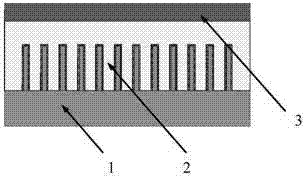
[0028] Step 1: The soft film plate with high aspect ratio flexible nano-cilia structure uses PDMS as the casting material, and performs the first film molding on the template of silicon-based nano-cilia structure. The specific process is as follows:

[0029] (a) adopt the passivation process in the high-density plasma etching to process the silicon-based nano-cilia array to carry out surface hydrophobicity treatment, and its specific process is as follows: C 4 f 8 The gas flow rate is 85sccm, the power of the lower plate is 600W, and the APC valve is 82%. After a 1-minute passivation process, the thickness of the fluorinated carbon deposited on the surface of the silicon-based nano-cilia array is about 150nm.

[0030] (b) Mix the PDMS solvent and curing agent (RTV615, GE Si...


PUM


Abstract

The invention belongs to the field of manufacturing integrated circuits and micro-nano electro-mechanical systems, in particular to a method for manufacturing a high-aspect-ratio nanostructure array. The method needs to prepare a soft template with a flexible nano-cilia structure with a high aspect ratio, and the soft film version uses PDMS as a casting material; the template for replicating a flexible nano-cilia array with a high aspect ratio is required. Using the embossed PDMS as a template, UV-curable adhesive OrmoStamp material is used for imprinting, so that the same flexible structure as on the silicon mold is obtained. The beneficial effect of the present invention is: aiming at the manufacturing difficulties of high aspect ratio flexible nanostructures, two flexible materials based on PDMS and ultraviolet light curing adhesive OrmoStamp are proposed, and the flexibility of high aspect ratio nanocilia arrays can be realized by two embossing methods. Fabrication, providing important technical support for the fabrication of high aspect ratio flexible nanostructures.

Description

[0001] Field [0002] The invention belongs to the field of manufacturing integrated circuits and micro-nano electro-mechanical systems, in particular to a method for manufacturing a high-aspect-ratio nanostructure array. Background technique [0003] Although silicon-based nanoarrays with high aspect ratios have been successfully manufactured, due to the very large elastic modulus of the silicon material itself (about 160 GP), in order to achieve low-frequency vibration detection, the absolute length of the silicon nano-cilia array must be increased to several hundred microns. This is not possible with the current processing technology. In order to solve this problem, we consider appropriately reducing the elastic modulus of the nano-cilia structure, thereby reducing the height of the nano-array, reducing the difficulty of etching, and realizing high-sensitivity detection of low-frequency acoustic signals. For this reason, it is necessary to study the fabrication of flexible ...

Claims


Application Information

Patent Timeline
Patent Type & Authority Patents(China)
IPC IPC(8): H01L21/02B82Y40/00G03F7/20
Inventor 马志波苑伟政姜澄宇乔大勇孟海莎
Owner NORTHWESTERN POLYTECHNICAL UNIV
Why Eureka
Try Eureka