Voltage conversion circuit

A voltage conversion circuit and circuit technology, applied in the field of circuits, can solve problems such as voltage instability

Active Publication Date: 2015-11-11
GIGADEVICE SEMICON (BEIJING) INC
View PDF5 Cites 3 Cited by
  • Summary
  • Abstract
  • Description
  • Claims
  • Application Information

AI Technical Summary

Problems solved by technology

[0003] However, the prior art will have the problem of voltage instability, which needs to be solved

Method used


Image

  • Voltage conversion circuit
  • Voltage conversion circuit
  • Voltage conversion circuit

Examples


Embodiment 1

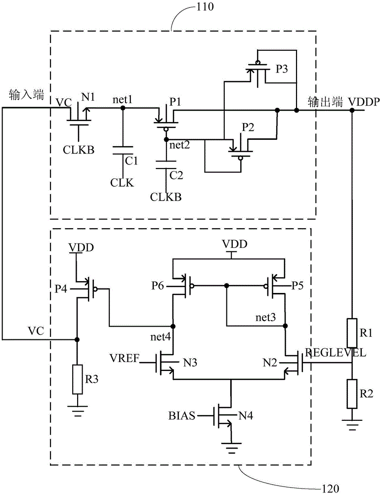
[0016] figure 1 It is a voltage conversion circuit diagram provided by Embodiment 1 of the present invention. This embodiment is applicable to the case where the load requires a supply voltage with a narrow variation range. A voltage conversion circuit diagram provided in this embodiment, such as figure 1 As shown, it includes: a first-order charge pump 110 and a negative feedback loop 120 .

[0017] The first-order charge pump 110 includes an input terminal, an output terminal, a forward clock control terminal (CLKB) and a reverse clock control terminal (CLK). Under the control of the provided clock signal, an output voltage is formed and output from the output terminal to provide voltage for the load.

[0018] The negative feedback loop 120 includes a power supply terminal, a voltage feedback terminal and a feedback output terminal, the voltage feedback terminal is connected to the output terminal of the first-order charge pump, and is used to adjust the source voltage inp...

Embodiment 2

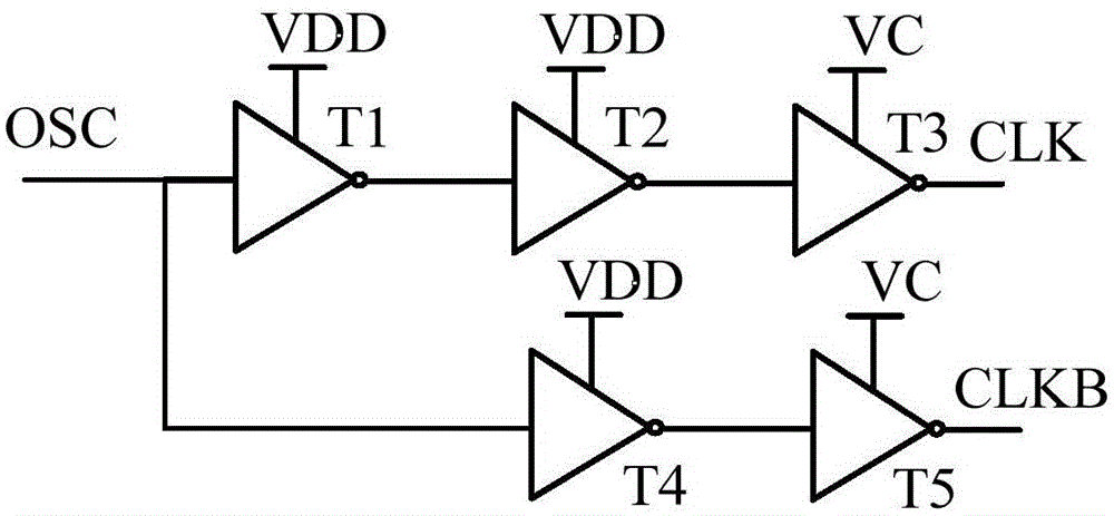
[0029] On the basis of the above examples, figure 2 It is the circuit diagram of the clock signal generator provided by Embodiment 2 of the present invention, such as figure 2 As shown, the input terminal of the clock signal generator is connected to the output terminal of an oscillator, and the output terminal is connected to the clock control terminal of the first-stage charge pump for adjusting the amplitude of the clock signal.

[0030] The clock signal processing circuit includes a first inverter T1, a second inverter T2, a third inverter T3, a fourth inverter T4 and a fifth inverter T5; wherein the first inverter , the second inverter and the third inverter are sequentially connected in series; the fourth inverter and the fifth inverter are connected in series with the first inverter, the second inverter and the third inverter devices in parallel.

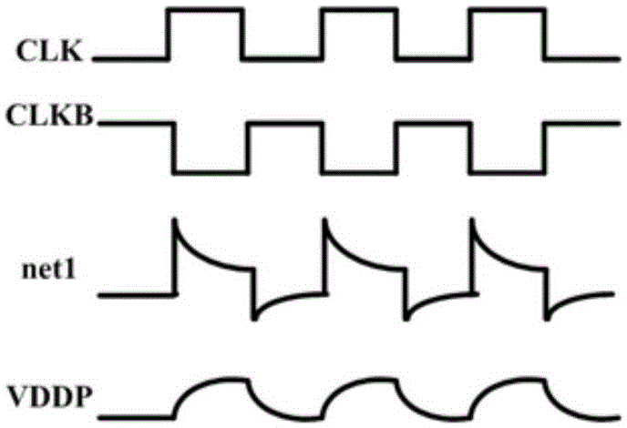
[0031] The amplitude of the clock signal is finally determined by the supply voltage VC of T3 and T5, such as figure ...


PUM


Abstract

The invention discloses a voltage conversion circuit. The voltage conversion circuit comprises a first order charge pump and a negative feedback loop, wherein the first order charge pump comprises an input terminal, an output terminal, a forward direction clock control terminal and a reverse direction clock control terminal; the first order charge pump is used for forming an output voltage and outputting the output voltage from the output terminal under the control of a clock signal provided by the forward direction clock control terminal and the reverse direction clock control terminal, and providing a voltage for a load; the negative feedback loop comprises a power supply terminal, a voltage feedback terminal and a feedback output terminal; the voltage feedback terminal is connected to the output terminal of the first order charge pump and is used for adjusting a source voltage input by the power supply terminal according to the output terminal so as to form a feedback voltage, and the feedback voltage is output from the feedback output terminal to an input terminal of the first order charge pump. In embodiments of the invention, the negative feedback loop controls an input voltage of the first order charge pump and an amplitude of the clock signal so that the input terminal voltage of the first order charge pump is transmitted to the output terminal and the stable output voltage is formed.

Description

technical field [0001] Embodiments of the present invention relate to circuit technology, and in particular to a voltage conversion circuit. Background technique [0002] Voltage conversion circuits are used to convert the voltage of a signal from one analog voltage range to another analog voltage range. [0003] However, there is a problem of voltage instability in the prior art, which needs to be solved. Contents of the invention [0004] The invention provides a voltage conversion circuit to output a stable target voltage. [0005] An embodiment of the present invention provides a voltage conversion circuit, including: a first-order charge pump, including an input terminal, an output terminal, a forward clock control terminal, and a reverse clock control terminal, and the first-order charge pump is used to control Under the control of the clock signal provided by the terminal and the reverse clock control terminal, the output voltage is output from the output terminal...

Claims


Application Information

Patent Timeline
Patent Type & Authority Applications(China)
IPC IPC(8): H02M3/07
Inventor 陈晓璐胡洪
Owner GIGADEVICE SEMICON (BEIJING) INC
Why Eureka
Try Eureka