Methods for connecting double-surface printed circuit board and welding electronic components by employing ultrasonic waves

A technology of ultrasonic welding and double-sided printing, which is applied in the direction of assembling printed circuits, electrical components, and printed circuits with electrical components, which can solve the problems of high price and many filling metal processes, achieve short welding time, and meet the utilization rate of space design. , the effect of not fragile metal properties

Inactive Publication Date: 2015-11-11
SHANGHAI AMPHENOL AIRWAVE COMM ELECTRONICS CO LTD
View PDF5 Cites 4 Cited by
  • Summary
  • Abstract
  • Description
  • Claims
  • Application Information

AI Technical Summary

Problems solved by technology

[0003] The conduction connection method of the double-sided printed circuit board is mainly through laser drilling or drilling and filling the hole with metal to connect the conduction. There are many processes for filling metal and the price is relatively high.

Method used


Image

  • Methods for connecting double-surface printed circuit board and welding electronic components by employing ultrasonic waves
  • Methods for connecting double-surface printed circuit board and welding electronic components by employing ultrasonic waves
  • Methods for connecting double-surface printed circuit board and welding electronic components by employing ultrasonic waves

Examples


Embodiment Construction

[0027] The present invention will be described in detail below in terms of specific embodiments in conjunction with the accompanying drawings. The following examples will help those skilled in the art to further understand the present invention, but do not limit the present invention in any form. It is to be noted that other embodiments may be utilized or structural and functional modifications may be made to the embodiments set forth herein without departing from the scope and spirit of the invention.

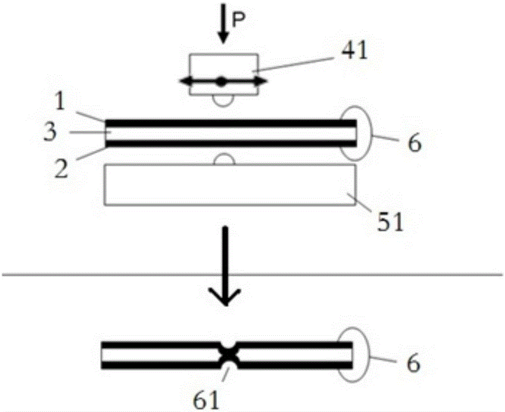
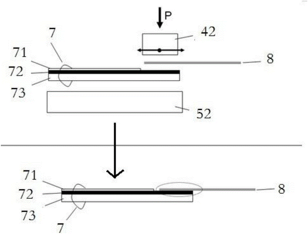
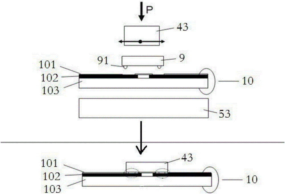
[0028] The object of the present invention is to provide a method for connecting double-sided printed circuit boards and soldering electronic components with ultrasonic waves. These two methods are all based on the same principle: high-frequency vibrations are generated on the contact surface of the workpiece through ultrasonic transmission, and high-frequency vibrations generate high-frequency vibrations. Density energy thus completes the welding between the two workpieces. ...


PUM


Abstract

The invention provides methods for connecting a double-surface printed circuit board and welding electronic components by employing ultrasonic waves. The method for connecting the double-surface printed circuit board includes: during conduction connection of the double-surface printed circuit board via the ultrasonic waves, an ultrasonic machine drives a welding fixture to perform parallel ultrasonic vibration on the surfaces of metal layers of the double-surface printed circuit board, when high-frequency vibration waves are transmitted to the metal surfaces at two sides of the double-surface printed circuit board via the welding fixture, the generated high-density energy gradually catalyzes a resin layer in the middle of the printed circuit board, the metal layers at two sides are inwardly recessed to be welded together, and the connecting effect is achieved. The method for welding the electronic components by employing the ultrasonic waves includes: the high-density energy generated by ultrasonic vibration waves of an ultrasonic welding fixture enables metal surfaces of two components to perform mutual friction so that the fusion between metal layers is formed, a firm combination is formed between the components, and the welding effect is achieved.

Description

technical field [0001] The invention relates to the field of circuit board manufacturing, in particular to a method for connecting double-sided printed circuit boards and welding electronic components by ultrasonic waves. Background technique [0002] At present, in the field of communication electronic products and equipment manufacturing, the most widely used welding methods between metal surfaces of electronic parts are solder paste welding, laser welding, reflow soldering and wave soldering. The space design and performance requirements of many electronic products will limit the area of ​​solder paste and the choice of soldering methods. [0003] The conduction connection method of the double-sided printed circuit board is mainly through laser drilling or drilling and filling the hole with metal to connect the conduction. There are many processes for filling metal and the price is relatively high. In order to reduce the soldering of components and the conduction of doub...

Claims


Application Information

Patent Timeline
Patent Type & Authority Applications(China)
IPC IPC(8): H05K3/34
CPCH05K3/341H05K2203/0285
Inventor 陈德智邹继鸿蒋海英
Owner SHANGHAI AMPHENOL AIRWAVE COMM ELECTRONICS CO LTD
Why Eureka
Try Eureka