Supercharge Your Innovation With Domain-Expert AI Agents!

An electrostatic protection circuit

An electrostatic protection and circuit technology, applied in the field of electrostatic protection circuits, can solve the problems of lower trigger voltage, etc., and achieve the effects of low trigger voltage, reduced risk of latch-up effect, and fast response speed

Active Publication Date: 2018-06-29
WUHAN XINXIN SEMICON MFG CO LTD
View PDF3 Cites 0 Cited by
  • Summary
  • Abstract
  • Description
  • Claims
  • Application Information

AI Technical Summary

Problems solved by technology

The reverse breakdown voltage of N+ / PW is much lower than that of NW / PW, which makes the trigger voltage of LVTSCR lower than that of traditional SCR

Method used


Image

  • An electrostatic protection circuit
  • An electrostatic protection circuit
  • An electrostatic protection circuit

Examples


Embodiment Construction

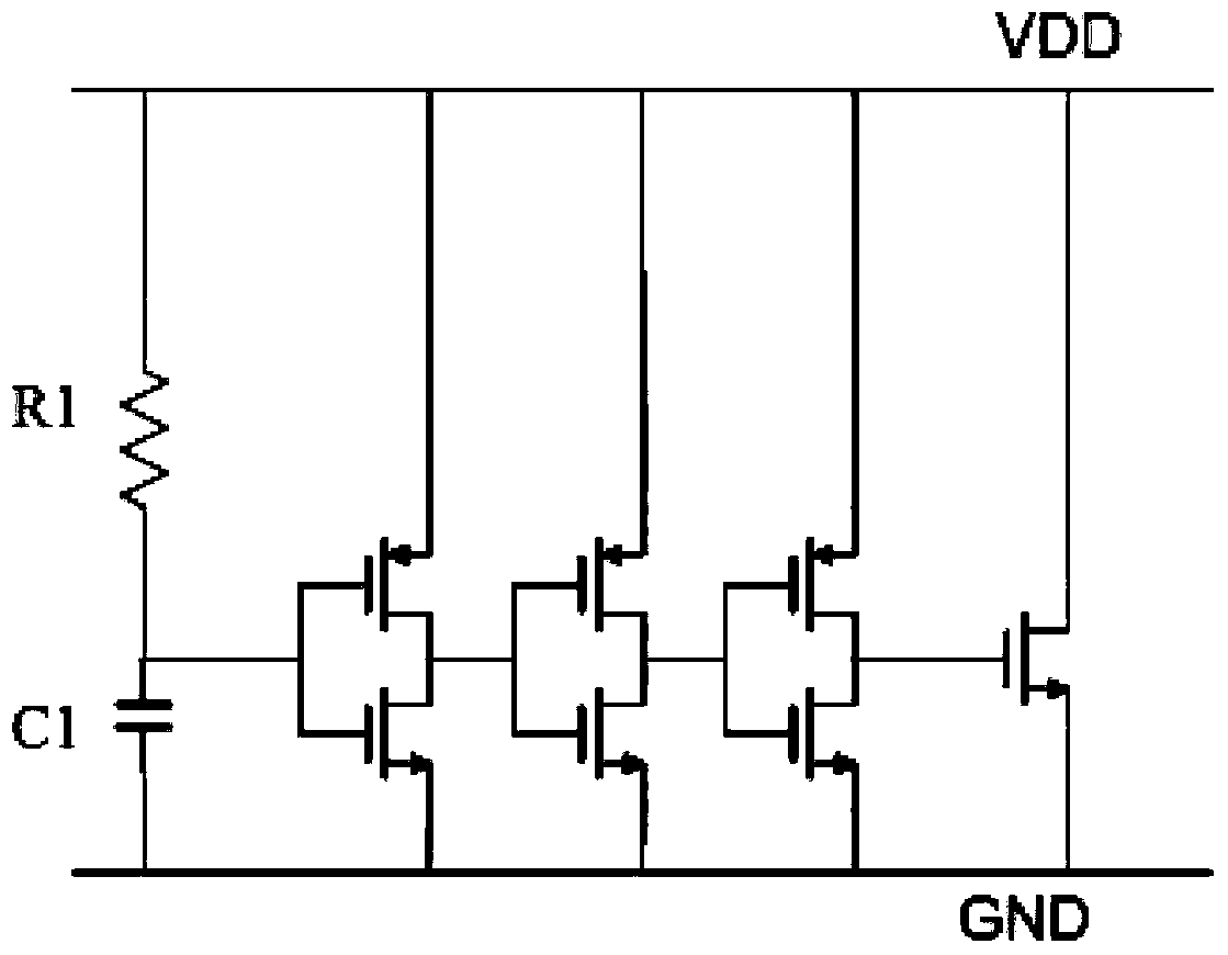
[0037] refer to Figure 4 The structure shown is an electrostatic protection circuit in an embodiment of the present invention. Specifically, the electrostatic protection circuit mainly includes: a trigger module 1 , a current mirror module 2 and an SCR module 3 . in:

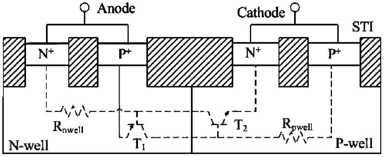
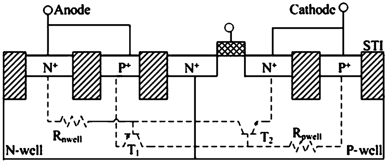
[0038] The SCR module 3 includes a first resistor Rnwell connected in series, an NPN transistor T2, a PNP transistor T1 connected in series, and a second resistor Rpwell, one end of the first resistor Rnwell is connected to the first reference voltage, and one end of the first resistor Rnwell is connected to the first reference voltage. The opposite end and the base of the PNP transistor T1 are commonly connected to the collector of the NPN transistor T2, one end of the second resistor Rpwell is connected to the second reference voltage, and the other end of the second resistor Rpwell is connected to the NPN. The bases are commonly connected to the collector of the PNP transistor, the emitter of the NPN transi...


PUM


Abstract

The present invention relates to the technical field of circuit electronics, in particular to an electrostatic protection circuit. By constructing an electrostatic protection circuit including a trigger module, a current generating unit and an SCR module, when VDD has a positive ESD pulse, the RC coupling effect makes the first NMOS The gate of the tube becomes high level, generating the first current from VDD to the first PMOS tube, the first NMOS tube to GND, the second PMOS tube is turned on, and the second current is generated to turn on the NPN triode transistor, and the NPN The collector current of the triode transistor flows through the first resistor so that the emitter-base of the PNP triode transistor is forward-biased, and the PNP triode transistor is turned on. This positive feedback effect makes the SCR formed by the PNP triode transistor and the NPN triode transistor open. discharge. The technical scheme has low trigger voltage and fast response speed, and the circuit can realize very good ESD protection performance with only a small size.

Description

technical field [0001] The invention relates to the technical field of circuit electronics, in particular to an electrostatic protection circuit. Background technique [0002] The problem of Electrostatic discharge (ESD) becomes more and more serious in IC products as the nodes become smaller. Commonly used ESD protection devices include MOS, DIODE, and SCR. Among them, SCR unit size has the strongest ESD protection ability. figure 1 It is a commonly used NMOS-based ESD protection structure. Using the characteristics of RC coupling, when there is a positive ESD pulse on VDD, the RC coupling effect makes the gate of the last NMOS high, and the NMOS starts to discharge. The disadvantage is that the discharge capacity per unit size of NMOS is relatively poor, and this circuit design requires a very large discharge NMOS transistor. Due to the large size of the NMOS, a three-stage inverter structure is required in the front stage to ensure that the NMOS can be turned on and d...

Claims


Application Information

Patent Timeline
Patent Type & Authority Patents(China)
IPC IPC(8): H02H9/04
Inventor 单毅
Owner WUHAN XINXIN SEMICON MFG CO LTD
Features
  • R&D
  • Intellectual Property
  • Life Sciences
  • Materials
  • Tech Scout
  • Unparalleled Data Quality
  • Higher Quality Content
  • 60% Fewer Hallucinations
Learn More