

Method of manufacturing buried word lines and isolating structures thereof
A technology of embedded word lines and isolation structures, which is applied in semiconductor/solid-state device manufacturing, electrical components, circuits, etc., can solve problems such as increased resistance, small component size, and impact on component performance, and achieve the effect of reducing interference
- Summary
- Abstract
- Description
- Claims
- Application Information
AI Technical Summary
Problems solved by technology
Method used
Image

Examples
Embodiment Construction
[0051] In order that the concept of the invention may be more fully appreciated, reference is made herein to the accompanying drawings, in which embodiments of the invention are shown. However, the invention may also be practiced in many different forms and should not be construed as limited to the embodiments set forth below. Rather, the embodiments are provided only so that the present disclosure will be thorough and complete, and will fully convey the scope of the present invention to those skilled in the art.
[0052] In the drawings, the size and relative sizes of layers and regions may be exaggerated for clarity.
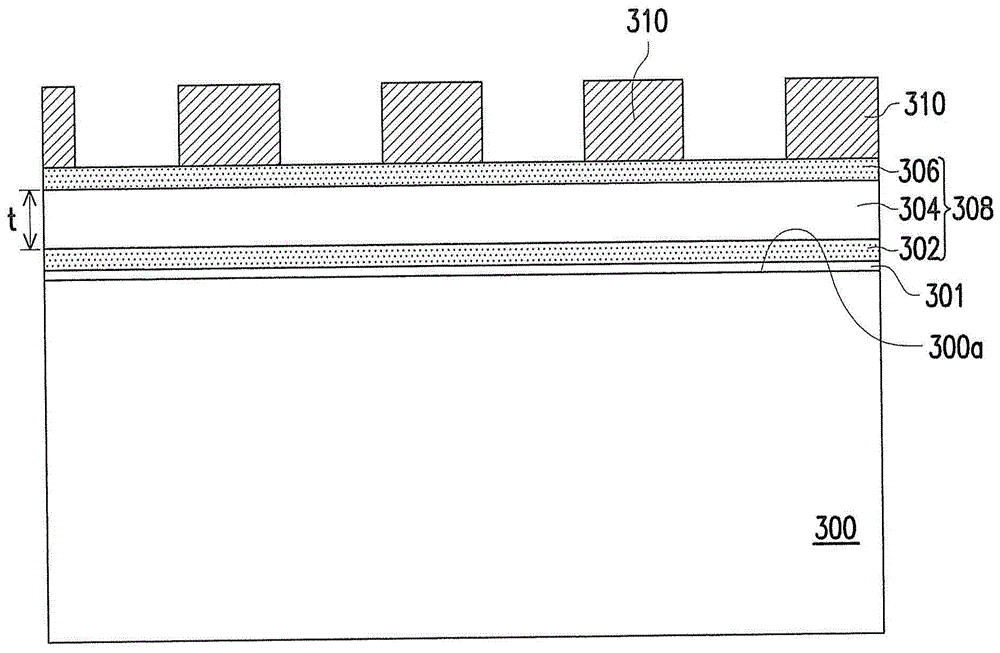
[0053] Figure 3A to Figure 3J It is a cross-sectional view of the manufacturing process of a buried word line and its isolation structure according to an embodiment of the present invention.
[0054] Please refer to Figure 3A A multi-layer structure 308 composed of a first nitride layer 302 , an oxide layer 304 and a second nitride layer 306 is formed on ...
PUM
 Abstract
Description
Claims
Application Information