


Quick Research
Generate reliable direction feasibility study reports for your R&D in just a few steps.

Technical Q&A
Discover and master advanced knowledge NOW. Basics, ideas, possibilities, all at once.

Find Solutions
As an expert in R&D theories, this can generate solutions to your technical problems instantly.

Evaluate Feasibility
Analyze your overall solution with one click, know your potential R&D risks in advance.

Monitor Landscape
Get weekly tech updates, stay abreast of the latest tech innovations and key insights.
Circuit board blind hole depth test structure and test method thereof
A technology of depth testing and testing methods, which is applied in electric/magnetic depth measurement, electromagnetic measurement devices, etc., can solve the problems of inability to obtain test results immediately on site, unfavorable long-term development of enterprises, limited number of slices, etc., and achieve convenient and fast testing. , Improve production efficiency and save the effect of slicing materials
- Summary
- Abstract
- Description
- Claims
- Application Information
AI Technical Summary
Problems solved by technology
Method used
Image

Examples
Embodiment 1
[0022] Embodiment 1 A kind of blind hole depth testing structure of two-layer circuit board
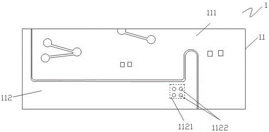
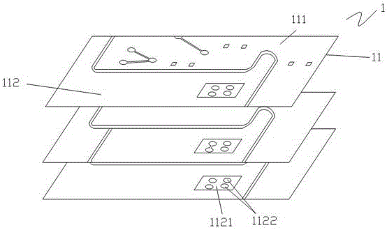
[0023] A circuit board blind hole depth test structure includes a circuit board body 1 to be drilled with blind holes formed by laminating three layers of circuit boards 11 . The three-layer circuit boards are provided with a line area 111 and an edge area 112 at the same position, and the line area and the edge area overlap after the three-layer circuit boards are laminated. The line area is the connecting circuit of the line, and the edge area is the area that needs to be removed during the edge process of the line. In the edge area 112 of each layer of circuit board, a depth test area 1121 for testing the circuit board to be drilled with blind holes is provided, and two groups of test points are arranged on the depth test area 1121 of each layer of circuit board 1122. The first group of test points indicates the connection status of the circuit board on the second layer, and the s...
Embodiment 2
[0024] Embodiment 2 A kind of testing method of blind hole depth of two-layer circuit board
[0025] A method for testing the depth of a blind hole on a circuit board, comprising the following specific steps:
[0026] S1. Select the three-layer circuit board body 1 made in Example 1 for testing.
[0027] S2. Place the circuit board body 1 on the platform of the drilling machine to drill holes. When drilling, the blind hole drilling knife and the test point drilling knife in the drilling machine move downward synchronously, and the depth of the downward movement is the same, so that the depth of the blind hole on the drilling knife and the test point on the circuit board body is the same as that of the test point. same depth. The drilling machine drills the blind holes in the circuit body and the two sets of test points on the circuit board. After drilling, clean the circuit board body to facilitate the next operation. The drilling machine can be drilled with a mechanical d...
Embodiment 3
[0034] Embodiment 3 A structure for testing the depth of blind holes in an N-layer circuit board
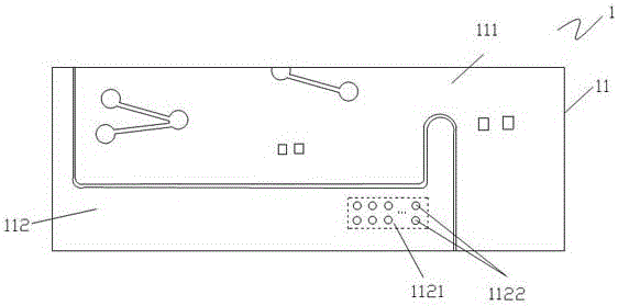
[0035]A circuit board blind hole depth test structure includes a circuit board body 1 formed by laminating N-layer circuit boards 11 to be drilled with blind holes. The line area 111 and the edge area 112 are provided at the same position of the N-layer circuit boards, and the line area and the edge area overlap after the N-layer circuit boards are laminated. The line area is the connecting circuit of the line, and the edge area is the area that needs to be removed during the edge process of the line. In the edge area 112 of each layer of circuit boards, a depth test area 1121 for testing circuit boards to be drilled with blind holes is provided, and N-1 groups are arranged on the depth test area 1121 of each layer of circuit boards. Test point 1122, the first group of test points indicates the connectivity of the second layer of circuit boards, the second group of test points i...
PUM
 Abstract
Description
Claims
Application Information
 - R&D Engineer
- R&D Manager
- IP Professional
- Industry Leading Data Capabilities
- Powerful AI technology
- Patent DNA Extraction
Browse by: Latest US Patents, China's latest patents, Technical Efficacy Thesaurus, Application Domain, Technology Topic, Popular Technical Reports.
© 2024 PatSnap. All rights reserved.Legal|Privacy policy|Modern Slavery Act Transparency Statement|Sitemap|About US| Contact US: help@patsnap.com