Liquid crystal display panel

A liquid crystal display panel and liquid crystal layer technology, applied in nonlinear optics, instruments, optics, etc., can solve the problems of reducing aperture ratio, increasing production cost, increasing material consumption, etc., and achieve the effect of improving contrast and preventing light leakage

Active Publication Date: 2015-12-02
TCL CHINA STAR OPTOELECTRONICS TECH CO LTD
View PDF10 Cites 7 Cited by
  • Summary
  • Abstract
  • Description
  • Claims
  • Application Information

AI Technical Summary

Problems solved by technology

like image 3 As shown, the LCD panel with figure 1 The difference of the liquid crystal display panel shown is that the black spacer 140 is arranged in the pixel opening area, so that the height of the black spacer 140 can be made very thick, reaching a thickness of 3.8 μm, and at the same time, the black spacer in the peripheral area is light-shielding The thickness of the layer 150 is also 3.8 μm, and the increase of the thickness of the black light-shielding layer 150 can avoid the risk of light leakage in the frame glue area of ​​the liquid crystal display panel, but since the black spacer 140 is black, setting it in the pixel opening area will reduce the aperture ratio, and at the same time Due to the increase in the thickness of the black spacer 140 and the black light-shielding layer 150, the amount of required materials increases, thereby causing an increase in production costs

Method used


Image

  • Liquid crystal display panel
  • Liquid crystal display panel
  • Liquid crystal display panel

Examples


Embodiment Construction

[0035] In order to further illustrate the technical means adopted by the present invention and its effects, the following describes in detail in conjunction with preferred embodiments of the present invention and accompanying drawings.

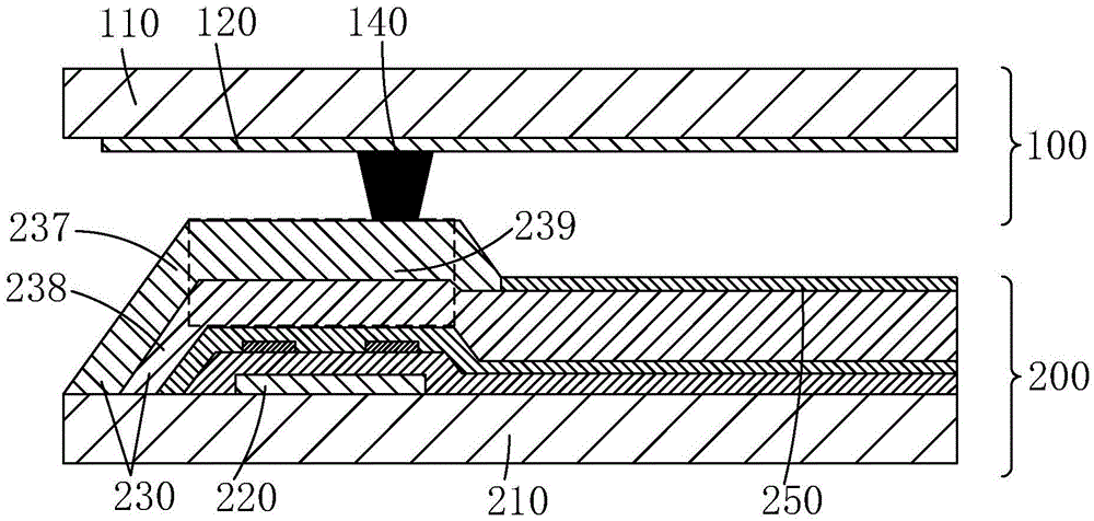
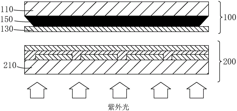
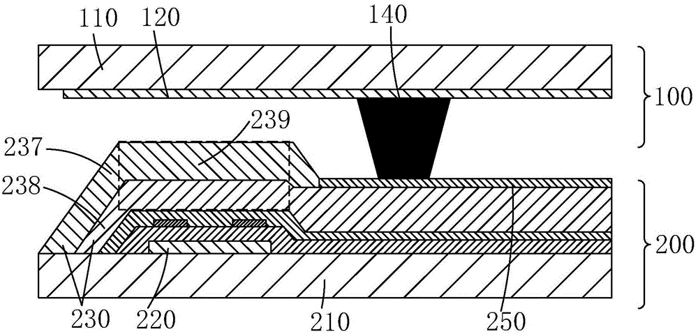
[0036] see Figure 5-6 , the present invention provides a liquid crystal display panel, comprising an upper substrate 1 and a lower substrate 2 arranged oppositely, and a liquid crystal layer arranged between the upper substrate 1 and the lower substrate 2;

[0037] Both the upper substrate 1 and the lower substrate 2 include a display area located in the middle and a peripheral area located on the periphery of the display area;

[0038] The upper substrate 1 includes a first substrate 11, a common electrode 12 disposed above the display area of ​​the first substrate 11, and a sealant 13 disposed above the peripheral area of ​​the first substrate 11;

[0039]The lower substrate 2 includes a second substrate 21, a gate scan line 22 disposed ab...


PUM

PropertyMeasurementUnit
Thicknessaaaaaaaaaa

Abstract

The invention provides a liquid crystal display panel. The two sides of a grid electrode scanning line are correspondingly provided with first light resistance blocks and second light resistance blocks. Both the first light resistance blocks and the second light resistance blocks extend towards the upper portion of the grid electrode scanning line, so that the extending portions of the first light resistance blocks and the extending portions of the second light resistance blocks are overlapped above the grid electrode scanning line, and an overlapped light resistance layer with a shielding effect is formed to replace a black matrix; meanwhile, a frame-shaped light resistance layer and a frame-shaped shielding layer made of black shielding materials are arranged at the position, corresponding to the position coated with frame glue of an upper substrate, on a lower substrate, the frame-shaped light resistance layer and the frame-shaped shielding layer jointly play the shielding function, the frame glue region of the liquid crystal display panel can be effectively prevented from leaking light, and therefore the contrast ratio of the liquid crystal display panel is increased.

Description

technical field [0001] The invention relates to the field of display technology, in particular to a liquid crystal display panel. Background technique [0002] A liquid crystal display device (LCD, Liquid Crystal Display) has many advantages such as a thin body, power saving, and no radiation, and has been widely used. Such as: LCD TV, mobile phone, personal digital assistant (PDA), digital camera, computer screen or laptop screen, etc. [0003] Generally, a liquid crystal display device includes a housing, a liquid crystal display panel disposed in the housing, and a backlight module disposed in the housing. Among them, the structure of the liquid crystal display panel is mainly composed of a thin film transistor array substrate (ThinFilmTransistorArraySubstrate, TFTArraySubstrate), a color filter substrate (ColorFilterSubstrate, CFSubstrate), and a liquid crystal layer (LiquidCrystalLayer) arranged between the two substrates. The principle is to control the rotation of t...

Claims


Application Information

Patent Timeline
IPC IPC(8): G02F1/1362G02F1/1339G02F1/1343
CPCG02F1/1339G02F1/13394G02F1/13439G02F1/1362G02F1/136209G02F1/136222
Inventor 叶成亮
Owner TCL CHINA STAR OPTOELECTRONICS TECH CO LTD
Why Eureka
Try Eureka