OLED film packaging structure, packaging method and display device

A technology of encapsulation structure and encapsulation method, which is applied to photovoltaic power generation, electrical components, circuits, etc., can solve the problems of easy breakage and poor bending resistance of the encapsulation part of flexible OLED devices, and achieve the effect of ensuring bending resistance.

Inactive Publication Date: 2015-12-02
TCL CHINA STAR OPTOELECTRONICS TECH CO LTD
View PDF3 Cites 16 Cited by
  • Summary
  • Abstract
  • Description
  • Claims
  • Application Information

AI Technical Summary

Problems solved by technology

[0004] Because the thickness of the overall thin-film package is on the order of microns, and the stress is relatively large when the inorganic film is thick, it is easy to break when it is bent, and water and oxygen will pass through this break to age the OLED device, making the bending resistance of the flexible OLED device package part change. Difference

Method used


Image

  • OLED film packaging structure, packaging method and display device
  • OLED film packaging structure, packaging method and display device
  • OLED film packaging structure, packaging method and display device

Examples


Embodiment Construction

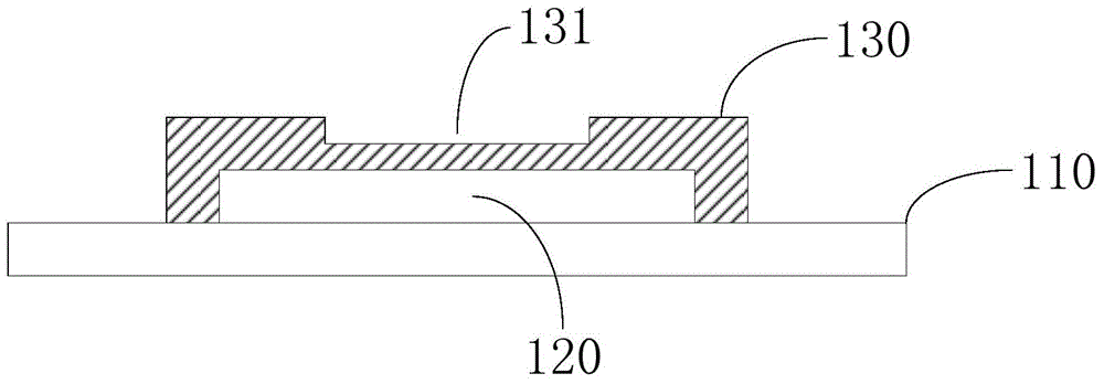
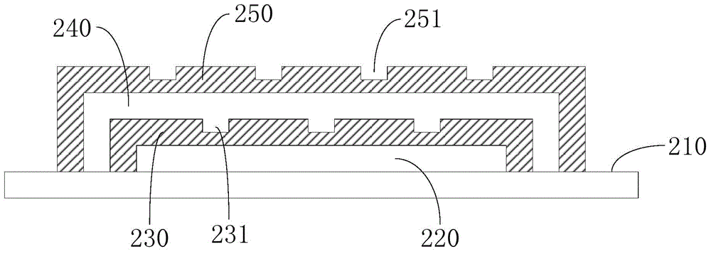
[0027] refer to figure 1 , a structural schematic diagram of the first embodiment of the OLED device packaging structure of the present invention, the packaging structure includes: a base substrate 110; an OLED device 120 located on the base substrate 110; a first passivation layer 130 covering the OLED device 120; wherein, The side of the first passivation layer 130 away from the OLED device 120 includes at least one thinning region 131 , the thickness of the thinning region 131 is smaller than the thickness of the first passivation layer 130 .

[0028] Wherein, the base substrate 110 is generally a glass substrate, and a bendable plastic substrate may also be used when making a flexible OLED panel.

[0029] The OLED device 120 includes an anode, a cathode, and an electroluminescent material between the anode and the cathode. When the anode and the cathode are energized, the luminescent material emits light for display.

[0030] The first passivation layer 130 is generally m...


PUM


Abstract

The invention discloses an OLED film packaging structure, a packaging method and a display device. The packaging structure comprises a substrate pedestal, an OLED device located on the substrate pedestal, and a first passivation layer covering the OLED device. One face, far away from the OLED device, of the first passivation layer comprises at least a thinning region, and the thickness of the thinning region is less than the thickness of the first passivation layer. The bending performance of a packaging part of a flexible OLED device can be enhanced.

Description

technical field [0001] The invention relates to the field of organic electroluminescence display, in particular to an OLED thin film packaging structure, a packaging method and a display device. Background technique [0002] Organic Light-Emitting Diode (OLED), also known as Organic Light-Emitting Diode (OLED), is a new generation of display. By making an organic thin film on an OLED substrate, the organic thin film is wrapped between the cathode and anode metals to add light to the two electrodes. voltage, the organic film will emit light. OLED displays have many advantages, including enabling flexible displays. For example, using a bendable plastic substrate as a carrier, combined with a thin film packaging process, a bendable OLED panel can be realized. [0003] At present, OLED thin-film packaging mainly adopts the structure of passivation layer and buffer layer stacking. The passivation layer is generally made of inorganic materials, such as SiNx; the buffer layer is ...

Claims


Application Information

Patent Timeline
Patent Type & Authority Applications(China)
IPC IPC(8): H01L51/52H01L51/56H01L27/32
CPCH10K59/00H10K50/84H10K71/00Y02E10/549H10K50/8445H10K2102/311H10K2102/351H10K77/111
Inventor 余威
Owner TCL CHINA STAR OPTOELECTRONICS TECH CO LTD
Why Eureka
Try Eureka