An array substrate and its preparation method, display panel and display device

An array substrate and substrate substrate technology, which is applied in semiconductor/solid-state device manufacturing, instruments, semiconductor devices, etc., can solve problems such as ESD on metal blocks or metal wires, avoid electrostatic discharge, improve product yield, and increase product yield. The effect of high tolerance

Active Publication Date: 2019-01-15
BOE TECH GRP CO LTD +1
View PDF4 Cites 0 Cited by
  • Summary
  • Abstract
  • Description
  • Claims
  • Application Information

AI Technical Summary

Problems solved by technology

[0003] In order to solve the above problems, the present invention provides an array substrate and its preparation method, a display panel and a display device, which are used to solve the problem of ESD occurring between metal blocks or metal lines of the array substrate in the prior art

Method used


Image

  • An array substrate and its preparation method, display panel and display device
  • An array substrate and its preparation method, display panel and display device
  • An array substrate and its preparation method, display panel and display device

Examples


Embodiment 1

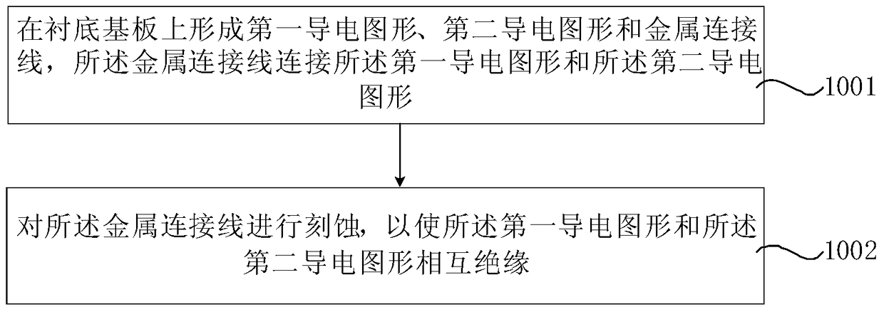
[0064] figure 1 It is a flow chart of a method for manufacturing an array substrate provided in Embodiment 1 of the present invention. Such as figure 1 As shown, the preparation method of the array substrate includes:

[0065] Step 1001 , forming a first conductive pattern, a second conductive pattern and a metal connection line on a base substrate, and the metal connection line connects the first conductive pattern and the second conductive pattern.

[0066] In this embodiment, the first conductive pattern includes a first gate metal pattern, the second conductive pattern includes a second gate metal pattern, and the gate metal pattern includes a gate and a gate line.

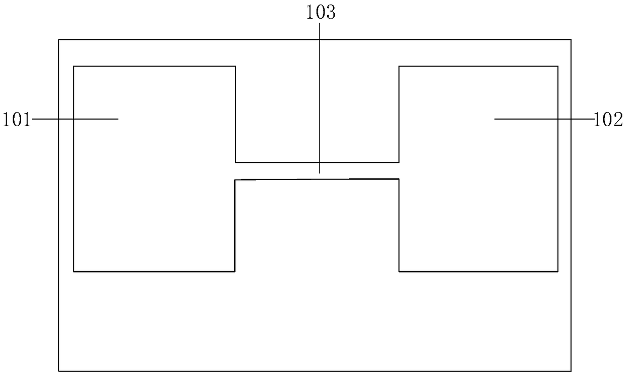
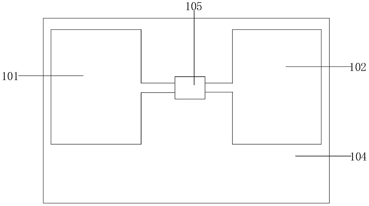
[0067] Figure 2a ~ Figure 2f It is a plan view of forming an array substrate in Embodiment 1, Figure 3a ~ Figure 3f for Figure 2a ~ Figure 2f Cross-sectional view corresponding to plan view shown. Such as Figure 2a ~ Figure 2f with Figure 3a ~ Figure 3f As shown, a first gate metal pattern 101, a ...

Embodiment 2

[0074] This embodiment provides a method for preparing an array substrate. see figure 1 , the preparation method comprises:

[0075] Step 1001 , forming a first conductive pattern, a second conductive pattern and a metal connection line on a base substrate, and the metal connection line connects the first conductive pattern and the second conductive pattern.

[0076] In this embodiment, the first conductive pattern includes a first gate metal pattern, the second conductive pattern includes a second gate metal pattern, and the gate metal pattern includes a gate and a gate line.

[0077] Figure 4a ~ Figure 4f A plan view of the array substrate formed for Embodiment 2, Figure 5a ~ Figure 5f for Figure 4a ~ Figure 4f Cross-sectional view corresponding to plan view shown. Such as Figure 4a ~ Figure 4f with Figure 5a ~ Figure 5f As shown, a first gate metal pattern 101, a second gate metal pattern 102, and a metal connection line 103 are formed on the base substrate, and...

Embodiment 3

[0084] This embodiment provides a method for preparing an array substrate. see figure 1 , the preparation method comprises:

[0085] Step 1001 , forming a first conductive pattern, a second conductive pattern and a metal connection line on a base substrate, and the metal connection line connects the first conductive pattern and the second conductive pattern.

[0086] In this embodiment, the first conductive pattern includes a source metal pattern, the second conductive pattern includes a drain metal pattern, the source metal pattern includes a source electrode and a data line, and the drain metal pattern includes a drain metal pattern. pole.

[0087]In this embodiment, a gate metal pattern is formed on the substrate, and the gate metal pattern includes a gate and a gate line. A gate insulating layer and an active layer are formed on the gate metal pattern, and a first transparent electrode is formed on the active layer. A source metal pattern, a drain metal pattern and a m...


PUM


Abstract

The invention discloses an array substrate and a preparation method thereof, a display panel and a display device. The preparation method includes: forming a first conductive pattern, a second conductive pattern and a metal connection line on a base substrate, and the metal connection line Connecting the first conductive pattern and the second conductive pattern; etching the metal connecting line to insulate the first conductive pattern and the second conductive pattern from each other. The metal connection wire provided by the present invention connects the first conductive pattern and the second conductive pattern to balance the potential difference between the first conductive pattern and the second conductive pattern in the process, thereby reducing the occurrence probability of electrostatic discharge phenomenon in the process and improving Product yield.

Description

technical field [0001] The present invention relates to the field of display technology, in particular to an array substrate and a preparation method thereof, a display panel and a display device. Background technique [0002] In the Thin Film Transistor-Liquid Crystal Display (TFT-LCD) industry, High Advanced Super Dimension Switch (HADS) has the characteristics of high aperture ratio and is widely used in small-sized products in the production process. However, the display panel in the HADS mode has a problem of Electro-Static discharge (ESD for short). The occurrence of ESD is related to the potential difference between the metal lines. During the manufacturing process of the array substrate, due to equipment static electricity, frictional static electricity or process discharge, etc., the metal blocks or metal lines that have been fabricated on the substrate will accumulate charges. Due to the circuit setup, the charges accumulated between the metal blocks or wires ha...

Claims


Application Information

Patent Timeline
Patent Type & Authority Patents(China)
IPC IPC(8): H01L21/77H01L27/12
CPCH01L27/1214H01L27/1259G02F1/136204H01L27/0288H01L27/124G02F1/134372H01L27/1203H01L29/41733H01L29/78606H01L29/78696
Inventor 张治超郭总杰刘正张小祥陈曦刘明悬
Owner BOE TECH GRP CO LTD
Why Eureka
Try Eureka