Pixel defining layer structure and manufacturing method thereof, display panel, and display apparatus

A pixel definition layer and display panel technology, applied in semiconductor/solid-state device manufacturing, electrical components, electric solid-state devices, etc., can solve the problems of pixel area reduction, crosstalk, ink overflow pixel pit color, etc., to achieve size reduction, The effect of increasing the deposition area

Inactive Publication Date: 2015-12-30
TCL CORPORATION
View PDF5 Cites 49 Cited by
  • Summary
  • Abstract
  • Description
  • Claims
  • Application Information

AI Technical Summary

Problems solved by technology

[0007] In view of the above deficiencies in the prior art, the object of the present invention is to provide a pixel defining layer structure and its manufacturing method, a display panel and a display device, aiming at solving the problem of the pixel area decrease caused by the increase of the resolution of the display device in the prior art. Small, which leads to the problem of ink overflowing pixel pits and causing color crosstalk

Method used


Image

  • Pixel defining layer structure and manufacturing method thereof, display panel, and display apparatus
  • Pixel defining layer structure and manufacturing method thereof, display panel, and display apparatus
  • Pixel defining layer structure and manufacturing method thereof, display panel, and display apparatus

Examples


Embodiment Construction

[0025] The present invention provides a pixel defining layer structure and its manufacturing method, a display panel and a display device. In order to make the object, technical solution and effect of the present invention clearer and clearer, the present invention will be further described in detail below. It should be understood that the specific embodiments described here are only used to explain the present invention, not to limit the present invention.

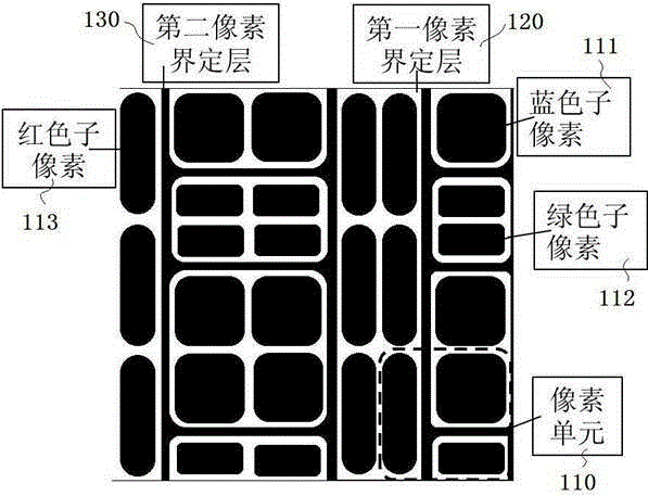
[0026] A pixel defining layer structure provided by the present invention, such as figure 1 As shown, it includes a first pixel defining layer and a second pixel defining layer 130 located on the first pixel defining layer 120, and the first pixel defining layer 120 has a structure compatible with each subpixel (eg figure 1 The blue sub-pixel 111, the green sub-pixel 112, and the red sub-pixel 113) have a plurality of first openings corresponding to each other, and the second pixel defining layer 130 has a region where th...


PUM


Abstract

The invention discloses a pixel defining layer structure and a manufacturing method thereof, a display panel, and a display apparatus. The pixel defining layer structure comprises a first pixel defining layer and a second pixel defining layer disposed on the first pixel defining layer, wherein the first pixel defining layer is provided with multiple first openings in one-to-one corresponding to the luminescence area of each sub pixel, and the second pixel defining layer is provided with multiple second openings shared by an area formed by connecting sub pixels having the same color. Through the pixel defining layer structure provided by the invention, the multiple sub pixels having the same color are combined together for simultaneous printing so that the deposition area of ink is increased by multiple times. Therefore, the dimension of each sub pixel can be effectively reduced, at the same time, it is ensured that the ink does not overflow due to too small area of the sub pixels, and finally, a printing type high-resolution display device is prepared.

Description

technical field [0001] The present invention relates to the field of display technology, in particular to a pixel defining layer structure and a manufacturing method thereof, a display panel and a display device. Background technique [0002] The use of solution processing to manufacture OLED and QLED displays is an important direction for the future development of display technology due to its advantages of low cost, high productivity, and easy realization of large sizes. Among them, printing technology is considered to be the most effective way to realize OLED and QLED low-cost and large-area full-color display. [0003] In the printing process, due to the influence of equipment precision and droplet size, it is difficult to realize the preparation of high-resolution display devices for the traditional RGBStripe (RGB strip) arranged pixel structure. When the resolution of the display device reaches 200ppi, the width of each sub-pixel will be reduced to 42μm. At the same t...

Claims


Application Information

Patent Timeline
Patent Type & Authority Applications(China)
IPC IPC(8): H01L27/32H01L21/77
Inventor 陈亚文付东
Owner TCL CORPORATION
Why Eureka
Try Eureka