Packaging substrate and manufacturing method thereof, and OLED display device and manufacturing method thereof

A technology for encapsulating substrates and manufacturing methods, which is applied in the direction of static indicators, semiconductor/solid-state device manufacturing, instruments, etc., can solve the problems of glass glue that cannot be cured, glass glue edge burrs, glass glue waste, etc., to improve the resistance to external water vapor and Oxygen intrusion ability, improvement of adhesion effect, effect of avoiding waste

Inactive Publication Date: 2016-01-06
BOE TECH GRP CO LTD +1
View PDF6 Cites 7 Cited by
  • Summary
  • Abstract
  • Description
  • Claims
  • Application Information

AI Technical Summary

Problems solved by technology

[0004] However, the inventors of the present application have found that, since the glass glue is viscous, the glass glue will flow outward after being applied to the packaging substrate, which will cause burrs on the edge of the glass glue
When irradiating the glass glue with laser, since the laser can only irradiate the glass glue in the bonding area, the glass glue in the area where the burr is located cannot be cured, and thus cannot play the role of bonding the display substrate and the packaging substrate, resulting in Waste of glass glue; at the same time, the part between the adjacent burrs on the outer edge of the glass glue is more susceptible to the invasion of external water vapor and oxygen, which seriously affects the life of the OLED display device

Method used


Image

  • Packaging substrate and manufacturing method thereof, and OLED display device and manufacturing method thereof
  • Packaging substrate and manufacturing method thereof, and OLED display device and manufacturing method thereof
  • Packaging substrate and manufacturing method thereof, and OLED display device and manufacturing method thereof

Examples


Embodiment Construction

[0029] The following will clearly and completely describe the technical solutions in the embodiments of the present invention with reference to the accompanying drawings in the embodiments of the present invention. Obviously, the described embodiments are some of the embodiments of the present invention, but not all of them. Based on the embodiments of the present invention, all other embodiments obtained by persons of ordinary skill in the art without making creative efforts belong to the protection scope of the present invention.

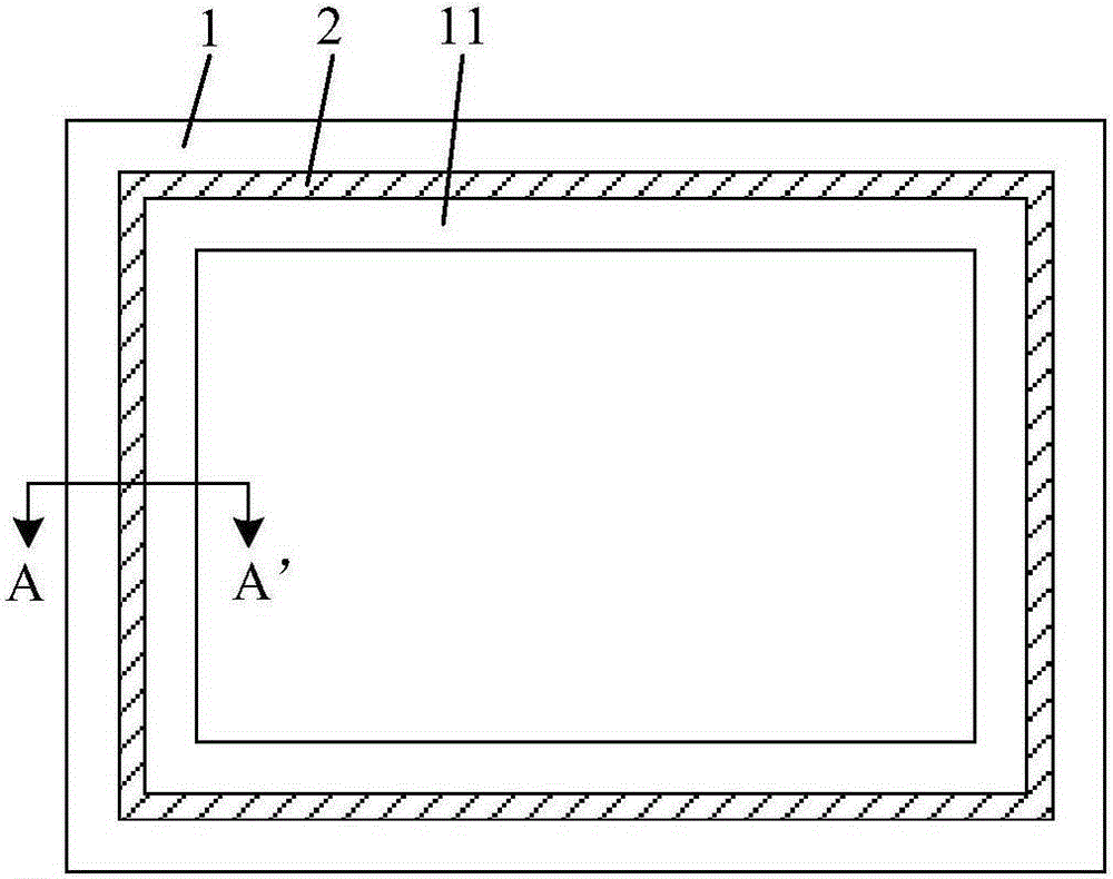
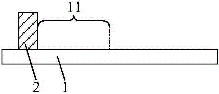
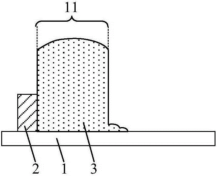
[0030] An embodiment of the present invention provides a packaging substrate, such as figure 1 and figure 2 As shown, the package substrate includes a base substrate 1, the base substrate 1 includes an adhesive area 11 for coating glass glue, and the package substrate also includes a first barrier wall 2 on the base substrate 1, the first barrier wall 2 is arranged along the outer edge of the bonding area 11, and the first retaining wall 2 is us...


PUM


Abstract

The invention discloses a packaging substrate and a manufacturing method thereof, an OLED display device and a manufacturing method thereof, relates to the technical field of display, and can prevent an outer side edge of glass cement coated on the packaging substrate from generating burrs. The packaging substrate includes a substrate, the substrate includes a bonding area used for coating glass cement, the packaging substrate also includes a first retaining wall located on the substrate, and the first retaining wall is arranged along an outer side edge of the bonding area and is used for stopping the glass cement coated on the bonding area from flowing outwards. The packaging substrate provided by the invention is used for preventing outside moisture and oxygen from entering an OLED display device.

Description

technical field [0001] The invention relates to the field of display technology, in particular to a packaging substrate and a manufacturing method thereof, an OLED display device and a manufacturing method thereof. Background technique [0002] Organic Light Emitting Display (OLED display for short) has gradually become the main development trend of display devices due to its advantages of self-luminescence, high brightness, high response speed, thinness, full color, and no viewing angle difference. [0003] The OLED display device includes a display substrate, on which a cathode, an anode, and an organic functional layer located between the cathode and the anode are arranged, wherein the organic functional layer is very sensitive to water vapor and oxygen, and is easily oxidized after contacting with water vapor or oxygen. lead to failure, thereby affecting the display effect of the OLED display device. In the prior art, the display substrate is packaged mainly through the...

Claims


Application Information

Patent Timeline
Patent Type & Authority Applications(China)
IPC IPC(8): H01L51/52H01S5/02315H01S5/0233
CPCH10K50/841H10K50/8426H01S5/0233H01S5/02315H01S5/0235H10K59/00G09G3/3208H01L33/641H01S5/42
Inventor 敖宁绰洛鹏闵天圭许瑾
Owner BOE TECH GRP CO LTD
Why Eureka
Try Eureka