Supercharge Your Innovation With Domain-Expert AI Agents!

Printed circuit board, package substrate, and method of fabricating the same

一种印刷电路板、封装基板的技术,应用在印刷电路制造、印刷电路、堆叠隔开印刷电路板等方向,能够解决焊裂、焊料坍塌、形成精细间距限制等问题,达到降低制造成本、提高可靠性、增强自由度的效果

Active Publication Date: 2016-01-06
LG INNOTEK CO LTD
View PDF5 Cites 3 Cited by
  • Summary
  • Abstract
  • Description
  • Claims
  • Application Information

AI Technical Summary

Problems solved by technology

[0014] However, since the first substrate and the second substrate are connected using solder balls 7, the prior art has a limit in forming fine pitches.
[0015] In addition, according to the prior art, problems such as solder cracks, solder bridges, and solder collapse may occur due to the use of solder balls 7

Method used


Image

  • Printed circuit board, package substrate, and method of fabricating the same
  • Printed circuit board, package substrate, and method of fabricating the same
  • Printed circuit board, package substrate, and method of fabricating the same

Examples


Embodiment Construction

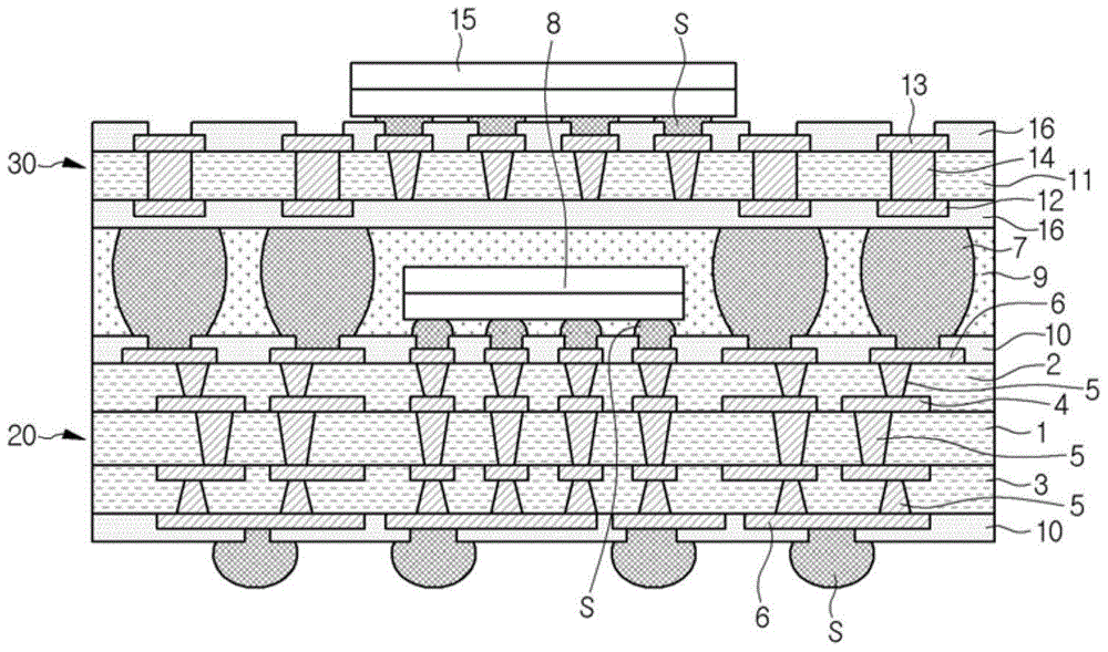
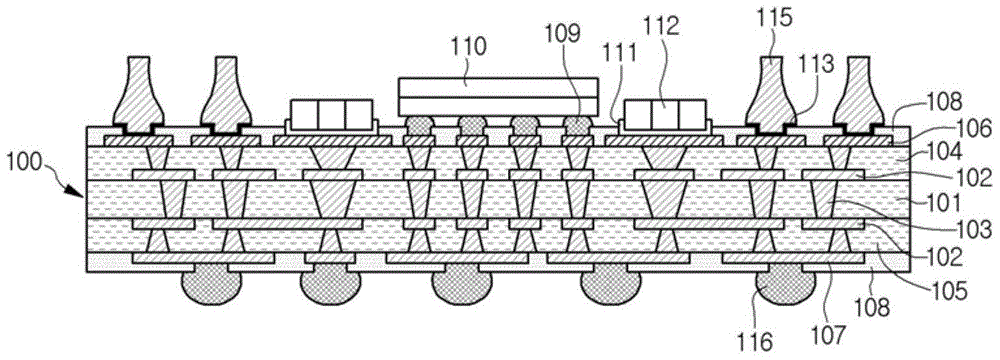
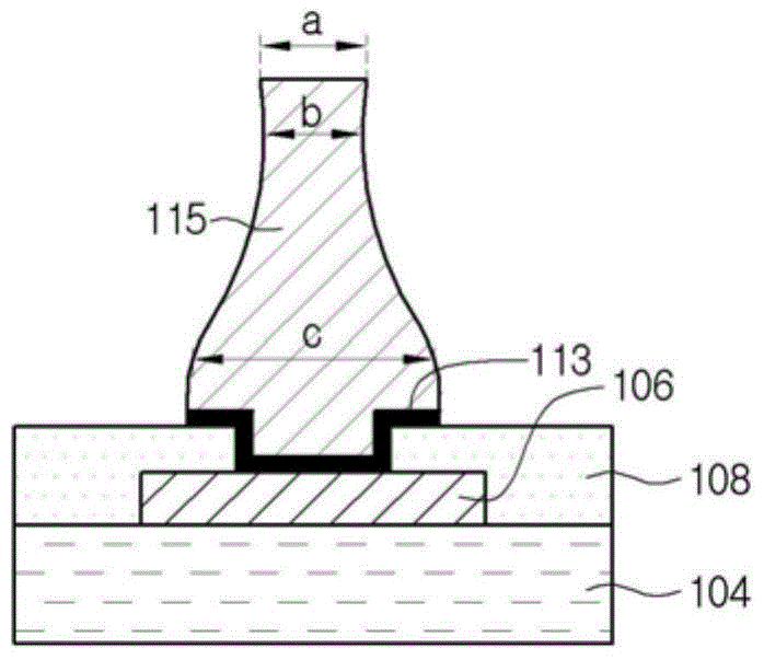
[0052] Hereinafter, the embodiments will be described in detail with reference to the accompanying drawings so that those skilled in the art can easily use the embodiments. However, the embodiments may have various modifications.

[0053] In the following description, when a predetermined component “includes” a predetermined component, the predetermined component does not exclude other components, but may further include other components, unless otherwise specified.

[0054] The thickness and size of each layer shown in the drawings may be exaggerated, omitted, or schematically drawn for convenience and clarity. In addition, the size of elements does not utterly reflect an actual size. Like reference numerals designate like elements throughout the drawings.

[0055] In describing embodiments, it will be understood that when a layer (or film), region, or panel is referred to as being "on" another element, it can be "directly" or "indirectly" on another element, Alternatively...


PUM


Abstract

A printed circuit board includes an insulating substrate, a plurality of pads on a top surface of the insulating substrate, a protective layer formed on the insulating substrate and having an opening to expose top surfaces of the pads, a bump formed on at least one of the pads and protruding upward of a surface of the protective layer. The bump has a curved lateral side.

Description

[0001] Cross References to Related Applications [0002] Pursuant to 35 U.S.C. § 119 and 35 § 365, this application claims priority to Korean Patent Application No. 10-2014-0080822 filed June 30, 2014, the entire contents of which are hereby incorporated by reference incorporated into this application. technical field [0003] The present embodiment relates to a printed circuit board, a packaging substrate and a manufacturing method thereof. Background technique [0004] Generally, the packaging substrate has a structure in which a first substrate to which a memory chip is attached is integrated with a second substrate to which a processor chip is attached. [0005] The package substrate is advantageous in that since the processor chip and the memory chip are integrated in the same package, the chip mounting area can be reduced and signals can be transmitted at a high rate. [0006] The package substrate is used in various mobile devices due to its advantages. [0007] f...

Claims


Application Information

Patent Timeline
Patent Type & Authority Applications(China)
IPC IPC(8): H05K1/11H01L21/48H01L23/498
CPCH01L21/486H01L23/49827H05K1/111H05K2201/0367H01L23/49822H01L24/13H01L24/16H01L24/81H01L25/105H01L25/50H01L2224/131H01L2224/16227H01L2224/81192H01L2225/1023H01L2225/1058H01L2924/1434H01L2924/15311H01L2924/15331H01L2924/181H01L2924/19041H01L2924/19042H01L2924/19043H01L2924/19105H05K1/144H05K3/4007H05K2201/042H05K2203/1383H01L2924/00012H01L2924/014H01L2924/00014
Inventor 金东先柳盛旭徐玄锡李知行
Owner LG INNOTEK CO LTD
Features
  • R&D
  • Intellectual Property
  • Life Sciences
  • Materials
  • Tech Scout
  • Unparalleled Data Quality
  • Higher Quality Content
  • 60% Fewer Hallucinations
Learn More