Method & apparatus for obtaining diagnostic information relating to a lithographic manufacturing process, lithographic processing system including diagnostic apparatus

a technology of lithographic manufacturing process and diagnostic equipment, applied in the direction of electrical equipment, instruments, material analysis, etc., can solve the problems of affecting the processing of other substrates in due time, the performance of subsequent processing steps, and the material of the substrate, so as to achieve the effect of automaticly obtaining diagnostic information much faster, maximizing yield and productivity, and better planning of maintenance operations

Active Publication Date: 2017-12-21
ASML NETHERLANDS BV
View PDF1 Cites 21 Cited by
  • Summary
  • Abstract
  • Description
  • Claims
  • Application Information

AI Technical Summary

Benefits of technology

[0012]By finding correlations between different types of measured data, the apparatus can automatically obtain diagnostic information much more quickly than the existing methods. The availability of this diagnostic information can allow better planning of maintenance operations to maximize yield and productivity. Where there is actually a need for an urgent intervention, this can be identified much more quickly. At the same time, unnecessary interventions for inspection and / or maintenance can be avoided, reducing downtime and extending component lifetimes. For example, early warning of contamination issues may allow certain maintenance operations to be brought forward into scheduled downtime rather than waiting until there is an emergency.

Problems solved by technology

Any of these handling operations can introduce defects to the substrate, which influence the performance of subsequent processing steps.
Defects may consist of damage to the material of the substrate, or particles of contaminant material adhering to the substrate.
Contamination can be transferred from a substrate to the substrate support or other handling apparatus, affecting processing of other substrates in due course.
Defects such as damage or contamination on the reverse side of the substrate can cause the substrate to be distorted.
However, defects of the type described above can introduce very localized height deviations, in other words curvature or “unflatness” of the substrate surface.
These deviations are not corrected by existing control systems.
Defects on a patterning device (mask or reticle) MA, may also arise and affect performance of the lithographic process.
Reticles are therefore subject to damage and contamination in the same way as the substrates to which the pattern is to be applied.
Distortion especially local curvature in the reticle can lead to loss of performance in overlay, CD etc. in the same way as local curvature of the substrate.
Consequently, a major problem for operators of lithographic manufacturing facilities is to detect and eliminate contamination or other defects as they affect yield.
On the other hand, to interrupt operations of the expensive equipment, whether for inspection or cleaning / replacement of parts, is extremely costly in itself.
Unnecessary maintenance operations are also costly, not only because of the interruption to productive operations, but also because they may reduce the lifetime of components.
Unfortunately, modern lithographic process and products are so complex that such issues are difficult to trace back to the root cause.
The analysis required to discover where such damage or contamination lies and / or where it originates can therefore be time consuming and difficult.
However, a typical defect map will show many features and most of these will not necessarily relate to detrimental effects in performance.
Also, to subject substrates to such inspection is costly and disruptive in itself, and may not be helpful if one does not know what one is looking for.
Some measurements are relatively easy and quick to obtain, but can make classifying the source of contamination difficult.
However, this data is not necessarily available without significant measurement overhead.
However, it is typically done by hand, by experts who carry out defect review sampling.
It may therefore take some time before appropriate action can be taken to counteract the contamination.
In a worst-case scenario, unplanned downtime may be required to deal with serious incidences of backside contamination.

Method used


Image

  • Method & apparatus for obtaining diagnostic information relating to a lithographic manufacturing process, lithographic processing system including diagnostic apparatus
  • Method & apparatus for obtaining diagnostic information relating to a lithographic manufacturing process, lithographic processing system including diagnostic apparatus
  • Method & apparatus for obtaining diagnostic information relating to a lithographic manufacturing process, lithographic processing system including diagnostic apparatus

Examples


Embodiment Construction

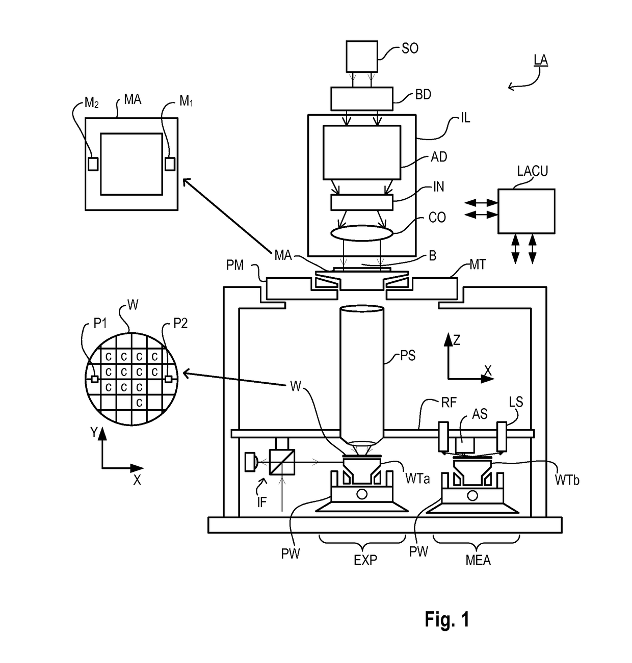
[0044]Before describing the techniques that are the specific subject of the present disclosure, it will be useful to present some background information on lithographic manufacturing processes and the issues arising therein. The examples will concern primarily processes for the production of functional devices on semiconductor substrates. The same principles can be applied to other types of product or substrates. It should also be appreciated in particular that the same principles can be applied in the manufacture of patterning devices such as reticles, which may themselves be used in a subsequent manufacturing process. Accordingly, references to the substrate in what follows may be construed also as references to a substrate on which a master pattern is to be formed, this being used subsequently for the applying functional device patterns to a series of substrates.

[0045]The patterning device can be an optical lithography reticle, either transmissive or reflective in type. The patte...


PUM

PropertyMeasurementUnit
defect sizeaaaaaaaaaa
clamping pressuresaaaaaaaaaa
wavelengthaaaaaaaaaa

Abstract

A diagnostic apparatus monitors a lithographic manufacturing system. First measurement data representing local deviations of some characteristic across a substrate is obtained using sensors within a lithographic apparatus, and/or a separate metrology tool. Other inspection tools perform substrate backside inspection to produce second measurement data. A high-resolution backside defect image is processed into a form in which it can be compared with lower resolution information from the first measurement data. Cross-correlation is performed to identify which of the observed defects are correlated spatially with the deviations represented in the first measurement data. A correlation map is used to identify potentially relevant clusters of defects in the more detailed original defect map. The responsible apparatus can be identified by pattern recognition as part of an automated root cause analysis. Alternatively, reticle inspection data may be used as second measurement data.

Description

CROSS-REFERENCE TO RELATED APPLICATIONS[0001]This application claims priority of EP application 14195683.9 which was filed on Dec. 1, 2014 and which is incorporated herein in its entirety by reference.BACKGROUNDField of the Invention[0002]The invention relates to a diagnostic apparatus for use in an industrial process. An example of an industrial process for which the apparatus has been developed is a lithographic manufacturing process, which includes one or more steps of transferring a pattern from a patterning device onto a substrate using a lithographic apparatus.Related Art[0003]A lithographic process is a manufacturing process in which the lithographic apparatus applies a desired pattern onto a substrate, usually onto a target portion of the substrate. The patterning step performed by the lithographic apparatus is just one step in a sequence of processing steps performed on each substrate in the entire lithographic process. The processing steps generally including one or more p...

Claims


Application Information

Patent Timeline
Patent Type & Authority Applications(United States)
IPC IPC(8): G03F7/20G01N27/61
CPCG03F7/70616G01N27/61G03F7/70508G01N21/9501G01N2021/95676G03F1/84G03F7/70783H01L22/12H01L22/20
Inventor HAUPTMANN, MARCDAVIES, DYLAN JOHN DAVIDJANSSEN, PAULTSUGAMA, NAOKOBRULS, RICHARD JOSEPHHOEKERD, KORNELIS TIJMENJANSSEN, EDWIN JOHANNES MARIAVAN DEN OEVER, PETRUS JOHANNESVAN DER WILK, RONALDVAN SCHIJNDEL, ANTONIUS HUBERTUSVIEYRA SALAS, JORGE ALBERTO
Owner ASML NETHERLANDS BV
Why Eureka
Try Eureka