Sorting mistake-proofing method and device for multiple layers of printed circuit board (PCB) lamination

An error-proofing and board-stacking technology, which is applied in multi-layer circuit manufacturing, electrical components, printed circuit manufacturing, etc., can solve problems such as flow to customers, failure to detect core board sorting errors, and loss of production costs.

Active Publication Date: 2016-01-06
DONGGUAN SHENGYI ELECTRONICS
View PDF5 Cites 5 Cited by
  • Summary
  • Abstract
  • Description
  • Claims
  • Application Information

AI Technical Summary

Problems solved by technology

At present, arranging and stacking multiple core boards in a specified order is done manually. During the stacking process, it is inevitable that there will be errors in the order due to human negligence.
In addition, the existing detection methods in the PCB industry cannot effectively detect the wrong sorting of core boards, making it difficult for problematic products to be found and flow to customers. They are only discovered when customers perform functional tests after mounting / packaging, which will lead to serious production cost loss
[0003] Based on the above situation, it is necessary for us to design an error-proof method to effectively monitor the sorting of the core boards during the stacking process to ensure that the wrongly sorted core boards are found before pressing, and to prevent the core boards from being unable to be reused after pressing. scrapped

Method used


Image

  • Sorting mistake-proofing method and device for multiple layers of printed circuit board (PCB) lamination
  • Sorting mistake-proofing method and device for multiple layers of printed circuit board (PCB) lamination
  • Sorting mistake-proofing method and device for multiple layers of printed circuit board (PCB) lamination

Examples


Embodiment Construction

[0069] The technical solutions of the present invention will be further described below in conjunction with the accompanying drawings and through specific implementation methods.

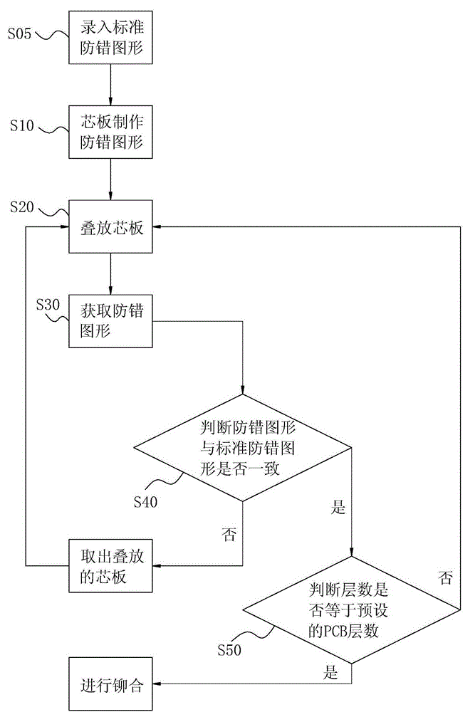
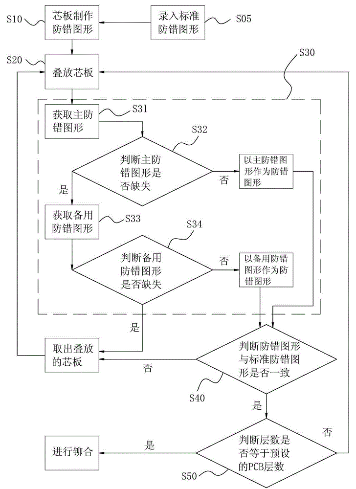
[0070] In this embodiment, if figure 1 and image 3 As shown, a sorting and error-proofing method for multilayer PCB stacks is provided, including the following steps:

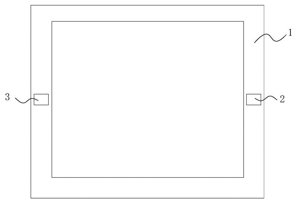
[0071] S10, making different error-proof graphics on core boards 1 of different levels;

[0072] S20, stacking one core board 1;

[0073] S30. Obtain the error-proofing pattern on the stacked core board 1;

[0074] S40. Judging whether the acquired error-proofing pattern is consistent with the standard error-proofing pattern of the corresponding level in the control system:

[0075] If not, take out the stacked core board 1, and return to step S20;

[0076] If yes, enter step S50;

[0077] S50, judging whether the number of layers of the core board 1 is equal to the number of pre-designed PCB layers:

[0078] If not, return t...


PUM


Abstract

The invention discloses a sorting mistake-proofing method for multiple layers of printed circuit board (PCB) lamination. The method comprises the following steps: fabricating different mistake-proofing patterns on different levels of core plates; stacking one core plate; obtaining the mistake-proofing pattern on the stacked core plate; judging whether the obtained mistake-proofing pattern is consistent with the corresponding level of standard mistake-proofing pattern in a control system or not, if so, taking out the stacked core plate, and restacking another core plate; if so, judging whether the number of layers of the core plates is equal to the number of layers of PCBs designed in advance or not, if not, stacking the next core plate; and if so, carrying out riveting. The invention further discloses a sorting mistake-proofing device for multiple layers of printed circuit board (PCB) lamination. The correctness of the mistake-proofing pattern on each core plate is judged in the plate stacking process to ensure that various core plates are stacked according to the specified order; according to the method, a riveting operation can be carried out only when the stacking orders of the core plates are all correct; and the core plate with a wrong stacking order is prevented from being riveted and fixed, so that scrapping and waste of the core plate are avoided.

Description

technical field [0001] The present invention relates to the technical field of PCB stacking technology, in particular to a multilayer PCB stacking method and device, and further relates to a multilayer PCB stacking error prevention method and device. Background technique [0002] Multi-layer PCB is formed by pressing multiple core boards in a specified order through high temperature and high pressure during the lamination process. At present, arranging and stacking multiple core boards in a specified order is done manually. During the stacking process, it is inevitable that there will be anomalies in the ordering errors due to human negligence. In addition, the existing detection methods in the PCB industry cannot effectively detect the wrong sorting of core boards, making it difficult for problematic products to be found and flow to customers. They are only discovered when customers perform functional tests after mounting / packaging, which will lead to serious loss of produ...

Claims


Application Information

Patent Timeline
Patent Type & Authority Applications(China)
IPC IPC(8): H05K3/46
CPCH05K3/4602H05K3/4611H05K2203/167
Inventor 陈仁喜柴绍东黄兵袁树华李光龙杨兴颜金雷邹艳丽许德勤
Owner DONGGUAN SHENGYI ELECTRONICS
Why Eureka
Try Eureka