How to make an LCD panel

A technology of liquid crystal panel and manufacturing method, applied in nonlinear optics, instruments, optics, etc., can solve problems such as unreasonable size installation module structure design, occurrence between black matrix and glass substrate, consumption cannot be underestimated, etc. , to achieve the effect of overcoming the peeling phenomenon, eliminating uneven brightness, and avoiding contact pollution

Active Publication Date: 2018-08-14
TCL CHINA STAR OPTOELECTRONICS TECH CO LTD
View PDF9 Cites 1 Cited by
  • Summary
  • Abstract
  • Description
  • Claims
  • Application Information

AI Technical Summary

Problems solved by technology

Although the material of the support 103 is a relatively low-cost consumable, as the production capacity of each factory continues to increase, the consumption should not be underestimated.
[0006] Finally, due to the current mainstream process conditions, the black matrix (Black Matrix, BM) 104 will be in direct contact with the glass substrate on the side of the CF substrate 100, and it is known from the analysis of the panels where the upper and lower substrates peel off (peeling) phenomenon, most of the Panel peeling occurs between the black matrix and the glass substrate, especially as the size of the panel increases and some installation modules are unreasonably designed.
The peeling of the upper and lower substrates will bring greater loss to the product, and research has found that the bonding strength between the sealant and the glass substrate is significantly higher than that between the black matrix and the glass substrate

Method used


Image

  • How to make an LCD panel
  • How to make an LCD panel
  • How to make an LCD panel

Examples


Embodiment Construction

[0043]In order to further illustrate the technical means adopted by the present invention and its effects, the following describes in detail in conjunction with preferred embodiments of the present invention and accompanying drawings.

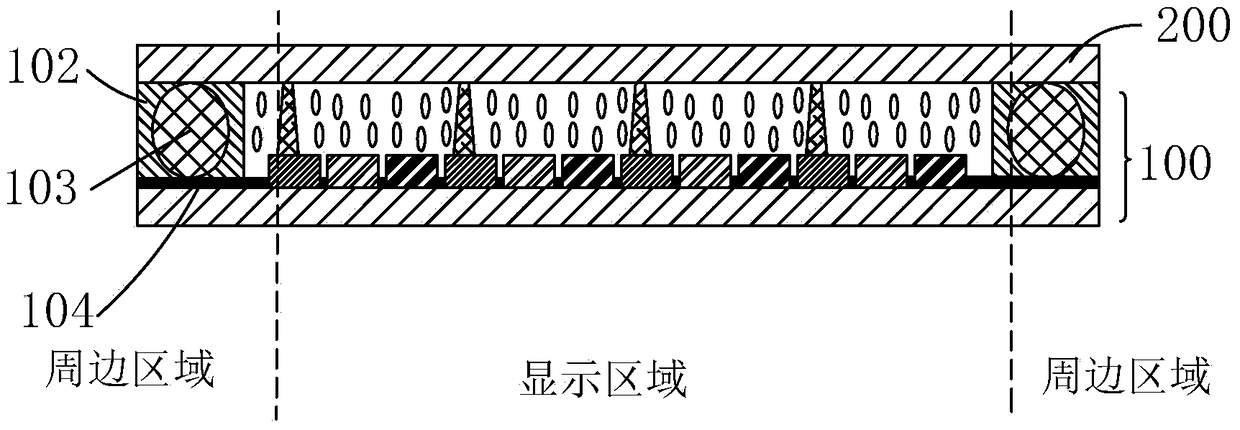
[0044] see Figure 3 to Figure 6 , the invention provides a method for manufacturing a liquid crystal panel, comprising the steps of:

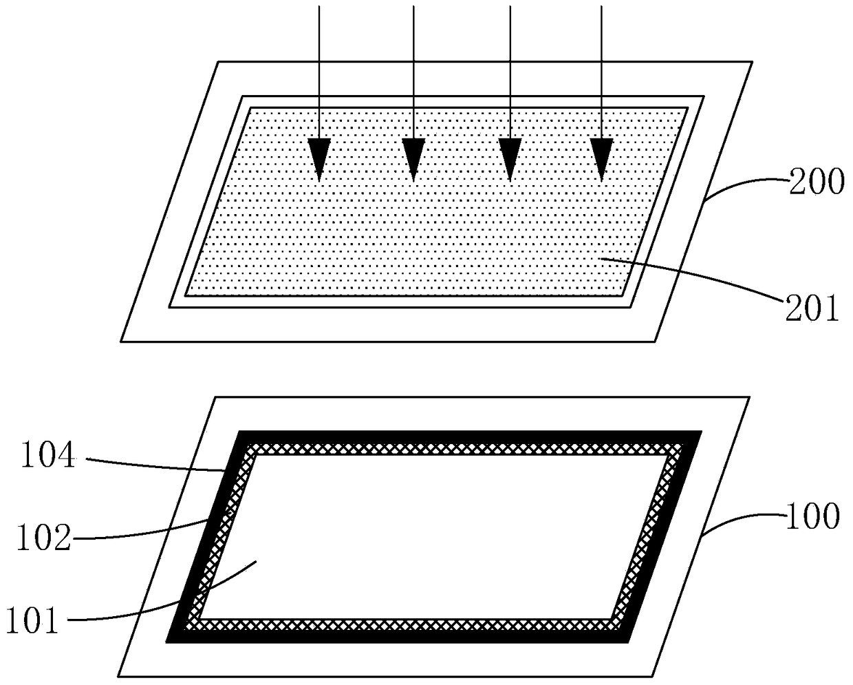
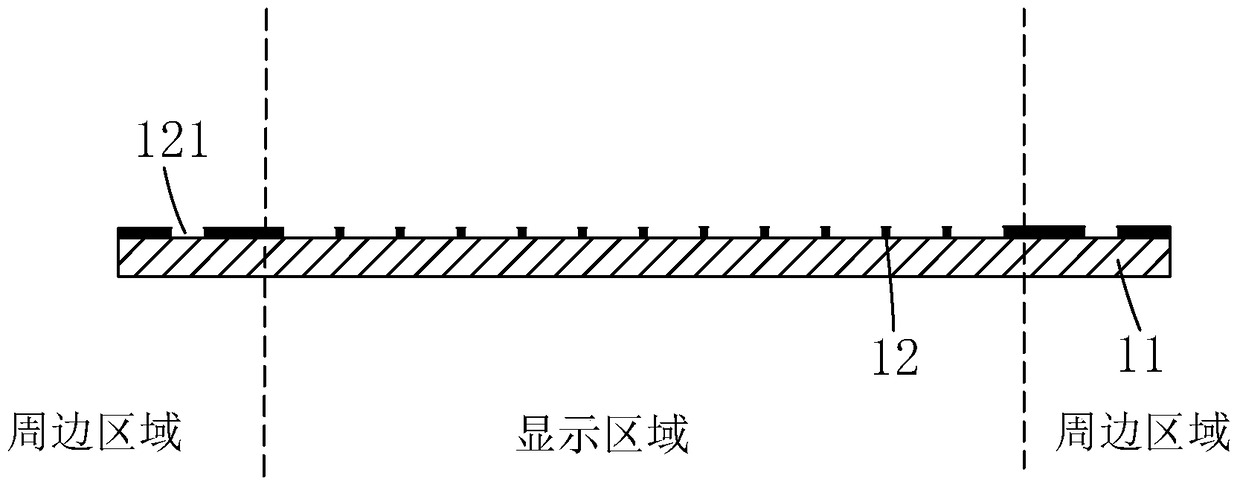
[0045] Step 1, such as image 3 As shown, a substrate 11 is provided, and the substrate 11 includes a display area and a peripheral area located at the periphery of the display area. Specifically, the substrate 11 is a glass substrate.

[0046] The black matrix material is coated on the substrate 11, and the black matrix material is exposed and developed through a photomask. While the black matrix 12 is formed, a groove 121 is formed on the black matrix 12 in the peripheral area to expose Substrate 11.

[0047] Step 2, such as Figure 4 As shown, red, green, and blue photoresist materials are sequentially ...


PUM

PropertyMeasurementUnit
optical densityaaaaaaaaaa

Abstract

The invention provides a manufacturing method for a liquid crystal display panel. According to the method, while black matrixes are formed, grooves are formed in black matrixes of peripheral areas; or while color blocking layers or spacers are formed, color blocking retaining walls or spacer retaining walls are formed on the black matrixes of the peripheral areas, a gluing area is formed between the grooves and the color blocking retaining walls or spacer retaining walls in a defined mode so as to isolate frame adhesive from a liquid crystal, and therefore the problem that due to contamination of contact between the frame adhesive and the liquid crystal, the peripheral areas of the liquid crystal display panel are uneven in brightness can be eliminated; the manufacturing process is simple, and an additional photomask and an additional exposure manufacturing process are not needed; the color blocking retaining walls or the spacer retaining walls can have an effect of supporting upper and lower substrates, and the production cost is reduced; in addition, as the grooves are formed in the black matrixes of the peripheral areas and filled with the frame adhesive, bonding force between the black matrixes and the upper and lower substrates is increased indirectly, and the stripping phenomenon is avoided; the width of the frame adhesive is adjustable, and therefore diversity requirements of narrow frame design are met.

Description

technical field [0001] The invention relates to the field of display technology, in particular to a method for manufacturing a liquid crystal panel. Background technique [0002] Thin Film Transistor-Liquid Crystal Display (TFT-LCD) includes a color filter substrate (Color Filter Substrate, CF Substrate,) and a thin film transistor array substrate (Thin Film Transistor Substrate, TFT Substrate), the substrate is relatively inner There are transparent electrodes. A layer of liquid crystal molecules (Liquid Crystal, LC) is sandwiched between the two substrates. The liquid crystal display controls the orientation of the liquid crystal molecules through the electric field, changes the polarization state of the light, and realizes the purpose of display by using the polarizer to realize the penetration and blocking of the light path. [0003] The CF substrate and the TFT substrate are combined by a sealant. The sealant is generally composed of acrylic, epoxy resin, photoinitiat...

Claims


Application Information

Patent Timeline
Patent Type & Authority Patents(China)
IPC IPC(8): G02F1/1335G02F1/1339G02F1/1333
CPCG02F1/1333G02F1/133512G02F1/1339
Inventor 马超
Owner TCL CHINA STAR OPTOELECTRONICS TECH CO LTD
Why Eureka
Try Eureka