Packaging method for image sensor chip and packaging structure

An image sensor chip and packaging method technology, which is applied to electrical components, electrical solid state devices, circuits, etc., can solve the problems of detachment and defectiveness of the pads 12 of the rewiring layer 24, and achieves improving the packaging yield, avoiding detachment, and improving The effect of reliability

Active Publication Date: 2016-01-13
CHINA WAFER LEVEL CSP
View PDF4 Cites 8 Cited by
  • Summary
  • Abstract
  • Description
  • Claims
  • Application Information

AI Technical Summary

Problems solved by technology

[0007] However, since the solder resist ink 26 fills the opening 22 , in the subsequent reflow soldering and reliability testing, the thermal expansion and contraction of the solder resist ink 26 forms a force acting on the rewiring layer 24 . , the rewiring layer 24 is easily detached from the pad 12, resulting in defects, which has become a technical problem to be solved by those skilled in the art

Method used


Image

  • Packaging method for image sensor chip and packaging structure
  • Packaging method for image sensor chip and packaging structure
  • Packaging method for image sensor chip and packaging structure

Examples


Embodiment Construction

[0031] Specific embodiments of the present invention will be described in detail below in conjunction with the accompanying drawings. However, these embodiments do not limit the present invention, and any structural, method, or functional changes made by those skilled in the art according to these embodiments are included in the protection scope of the present invention.

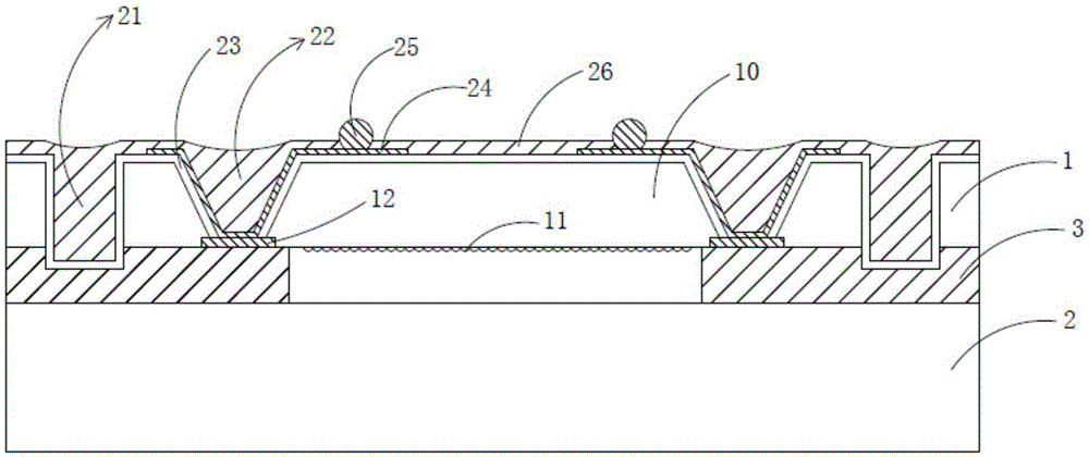
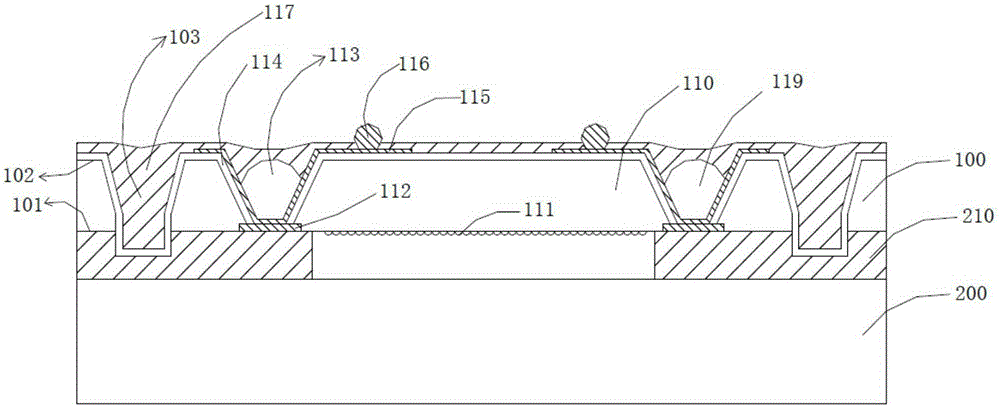
[0032] In the prior art, the solder resist ink fills the openings, so that the solder resist ink is in full contact with the rewiring layer, resulting in subsequent reflow soldering and reliability testing, the force formed by the shrinkage and expansion of the solder resist ink pulls the rewiring layer, which is easy to cause The redistribution layer is detached from the pad.

[0033] In order to solve the above problems, the present invention forms a cavity in the hole so that the solder resist ink does not contact the wiring layer at the bottom of the hole, which can effectively prevent the rewiring layer...


PUM


Abstract

The invention provides a packaging method for an image sensor chip and a packaging structure. The packaging method comprises the steps as follows: a wafer is provided; the wafer comprises a first surface and a second surface opposite to the first surface, and comprises the image sensor chip which is formed by arranging a plurality of grids; the image sensor chip comprises an image sensor region and a boning pad; the image sensor region and the boning pad are located on the first surface of the wafer; an opening which extends towards the first surface is formed in the second surface of the wafer, and exposes the bonding pad; a V-shaped cutting groove which extends towards the first surface is formed in the second surface of the wafer; a photosensitive ink coats the second surface of the wafer, so that the V-shaped cutting groove is fully filled with the photosensitive ink; the photosensitive ink covers the opening; and a hollow cavity is formed in the opening. The hollow cavity is formed in the opening, so that the condition that a re-wiring layer is separated from the bonding pad is effectively avoided; the packaging yield of the image sensor chip is improved; and the reliability of the packaging structure of the image sensor chip is improved.

Description

technical field [0001] The invention relates to the technical field of semiconductors, in particular to a packaging method for wafer-level semiconductor chips. Background technique [0002] Today's mainstream semiconductor chip packaging technology is Wafer Level Chip Size Packaging (WLCSP), which is a technology that packages and tests an entire wafer and then cuts it to obtain a single finished chip. The size of a single finished chip packaged by this packaging technology is almost the same as that of a single grain, which meets the market's increasingly light, small, short, thin and low-cost requirements for microelectronic products. Wafer-level chip-scale packaging technology is a hot spot in the current packaging field and a future development trend. [0003] Please refer to figure 1 , discloses a packaging structure of a wafer-level image sensor chip. A wafer 1 and a protective substrate 2 are aligned and pressed together, and a support unit 3 is located between the ...

Claims


Application Information

Patent Timeline
Patent Type & Authority Applications(China)
IPC IPC(8): H01L23/488H01L21/60
CPCH01L2224/11
Inventor 王之奇王卓伟谢国梁
Owner CHINA WAFER LEVEL CSP
Why Eureka
Try Eureka